
Datasheet


AD9549
Rev. D | Page 64 of 76
MONITOR (REGISTER 0x0300 TO REGISTER 0x0335)
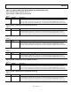
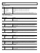
Register 0x0300—Status
This register contains the status of the chip. This register is read-only and live update.
Table 74.
Bits Bit Name Description
7 Reserved Reserved.
6 PFD frequency too high This flag indicates that the frequency estimator failed and detected a PFD frequency that is too high.
This bit is relevant only if the user is relying on the frequency estimator to determine the input
frequency.
5 PFD frequency too low This flag indicates that the frequency estimator failed and detected a PFD frequency that is too low.
This bit is relevant only if the user is relying on the frequency estimator to determine the input
frequency.
4 Frequency estimator done True when the frequency estimator circuit has successfully estimated the input frequency. See the
Frequency Estimator section.
3 Reference selected Reference selected.
0 = Reference A is active.
1 = Reference B is active.
2 Free run DPLL is in holdover mode (free run).
1 Phase lock detect This flag indicates that the phase lock detect circuit has detected phase lock. The amount of phase
adjustment is compared against a programmable threshold. Note that this bit can be set in single
tone and holdover modes and should be ignored in these cases.
0 Frequency lock detect This flag indicates that the frequency lock detect circuit has detected frequency lock. This feature
compares the absolute value of the difference of two consecutive phase detector edges against a
programmable threshold. Because of this, frequency lock detect is more rigorous than phase lock
detect, and it is possible to have phase lock detect without frequency lock detect.
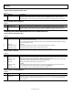
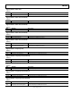
Register 0x0301—Status (Continued)
This register contains the status of the chip. This register is read-only and live update.
Table 75.
Bits Bit Name Description
7 Reserved Reserved.
6 REFA valid The reference validation circuit has successfully determined that Reference A is valid.
5 REFA LOR A LOR (loss of reference) has occurred on Reference A.
4 REFA OOL The OOL (out of limits) circuit has determined that Reference A is out of limits.
3 Reserved Reserved.
2 REFB Valid The reference validation circuit has successfully determined that Reference B is valid.
1 REFB LOR A LOR (loss of reference) has occurred on Reference B.
0 REFB OOL The OOL (out of limits) circuit has determined that Reference B is out of limits.
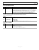
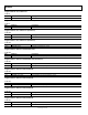
Register 0x0302 and Register 0x0303—IRQ Status
These registers contain the chip status (Registers 0x0300 and Register 0x0301) at the time of IRQ. These bits are cleared with an IRQ reset
(see Register 0x0012, Bit 5).
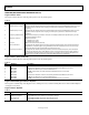
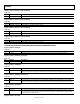
Register 0x0304—IRQ Mask
Table 76.
Bits Bit Name Description
[7:3] Reserved Reserved.
2 Reference changed Trigger IRQ when active reference clock selection changes.
1 Leave free run Trigger IRQ when DPLL leaves free-run (holdover) mode.
0 Enter free run Trigger IRQ when DPLL enters free-run (holdover) mode.