
Datasheet


AD9549
Rev. D | Page 63 of 76
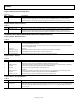
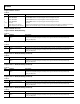
Register 0x01C3—Reference Validation
Table 71.
Bits Bit Name Description
[7:5] Reserved Reserved.
[4:0] Validation timer The value in this register sets the time required to validate a reference after an LOR or OOL event
before the reference can be used as the DPLL reference. This circuit uses the digital loop filter clock
(see Register 0x0107). Validation time = loop filter clock period × 2
(Validation Timer [4:0] +1)
− 1. Assuming
power-on defaults, the recovery time varies from 32 ns (00000) to 137 sec (11111). If longer valida-tion
times are required, the user can make the P-divider larger. The user should be careful to set the
validation timer to at least two periods of the OOL evaluation period. The OOL evaluation period is the
period of reference input clock times the OOL divider (Register 0x0322 to Register 0x0323).
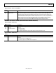
DOUBLER AND OUTPUT DRIVERS (REGISTER 0x0200 TO REGISTER 0x0201)
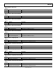
Register 0x0200—HSTL Driver
Table 72.
Bits Bit Name Description
4 OPOL Output polarity. Setting this bit inverts the HSTL driver output polarity.
[3:2] Reserved Reserved.
[1:0] HSTL output doubler HSTL output doubler.
01 = doubler disabled.
10 = doubler enabled. When using doubler, Register 0x0010[5] must also be set.
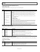
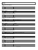
Register 0x0201—CMOS Driver
Table 73.
Bits Bit Name Description
0 CMOS mux User mux control. This bit allows the user to select whether the CMOS driver output is divided by the
S-divider.
0 = S-divider input sent to CMOS driver.
1 = S-divider output sent to CMOS driver. See Figure 22.