
Datasheet


AD9549
Rev. D | Page 54 of 76
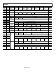
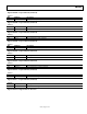
Register 0x0011—Reserved
Register 0x0012—Reset (Autoclear)
To reset the entire chip, the user can also use the (nonself-clearing) soft reset bit in Register 0x0000. Except for IRQ reset, the user normally
would not need to use this bit. However, if the user attempts to lock the loop for the first time when no signal is present, the user should
write 1 to Bits[4:0] of this register before attempting to lock the loop again.
Table 18.
Bits Bit Name Description
7 History reset Setting this bit clears the FTW monitor and pipeline.
6 Reserved Reserved.
5 IRQ reset Clear IRQ signal and IRQ status monitor.
4 FPFD reset Fine phase frequency detector reset.
3 CPFD reset Coarse phase frequency detector reset.
2 LF reset Loop filter reset.
1 CCI reset Cascaded comb integrator reset.
0 DDS reset Direct digital synthesis reset.
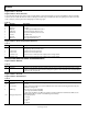
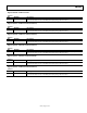
Register 0x0013—Reset (Continued) (Not Autoclear)
Table 19.
Bits Bit Name Description
7 PD fund DDS Setting this bit powers down the DDS fundamental output but does not power down the spurs. It is used
during tuning of the spur killer circuit.
3 S-div/2 reset Asynchronous reset for S prescaler.
2 R-div/2 reset Asynchronous reset for R prescaler.
1 S-divider reset Synchronous (to S-divider prescaler output) reset for integer divider.
0 R-divider reset Synchronous (to R-divider prescaler output) reset for integer divider.
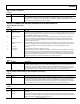
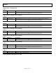
SYSTEM CLOCK (REGISTER 0x0020 TO REGISTER 0x0023)
Register 0x0020—N-Divider
Table 20.
Bits Bit Name Description
[4:0] N-divider These bits set the feedback divider for system clock PLL. There is a fixed/2 preceding this block, as well as
an offset of 2 added to this value. Therefore, setting this register to 00000 translates to an overall feedback
divider ratio of 4. See Figure 43.
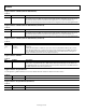
Register 0x0021—Reserved
Register 0x0022—PLL Parameters
Table 21.
Bits Bit Name Description
7 VCO auto range Automatic VCO range selection. Enabling this bit allows Bit 2 of this register to be set automatically.
[6:4] Reserved Reserved
3 2× reference Enables a frequency doubler prior to the SYSCLK PLL and can be useful in reducing jitter induced by the
SYSCLK PLL. See Figure 42.
2 VCO range Select low range or high range VCO.
0 = low range (700 MHz to 810 MHz).
1 = high range (900 MHz to 1000 MHz). For system clock settings between 810 MHz and 900 MHz, use the
VCO Auto Range (Bit 7) to set the correct VCO range automatically.
[1:0] Charge pump current Charge pump current.
00 = 250 μA.
01 = 375 μA.
10 = off.
11= 125 μA.