
Datasheet


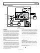

AD9549
Rev. D | Page 12 of 76
Pin No.
Input/
Output Pin Type Mnemonic Description
60 I 3.3 V CMOS IO_UPDATE I/O Update. A logic transition from 0 to 1 on this pin transfers data from the I/O
port registers to the control registers (see the Write section). This pin has an
internal 50 kΩ pull-down resistor.
61 I 3.3 V CMOS CSB Chip Select. Active low. When programming a device, this pin must be held
low. In systems where more than one AD9549 is present, this pin enables
individual programming of each AD9549. This pin has an internal 100 kΩ pull-
up resistor.
62 O 3.3 V CMOS SDO Serial Data Output. When the device is in 3-wire mode, data is read on this pin.
There is no internal pull-up/pull-down resistor on this pin.
63 I/O 3.3 V CMOS SDIO Serial Data Input/Output. When the device is in 3-wire mode, data is written
via this pin. In 2-wire mode, data reads and writes both occur on this pin. There
is no internal pull-up/pull-down resistor on this pin.
64 I 3.3 V CMOS SCLK Serial Programming Clock. Data clock for serial programming. This pin has an
internal 50 kΩ pull-down resistor.
Exposed
Die Pad
O GND EPAD Analog Ground. The exposed thermal pad on the bottom of the package pro-
vides the analog ground for the part. This exposed pad must be connected to
ground for proper operation.