
Datasheet


AD9517-4 Data Sheet
Rev. E | Page 14 of 80
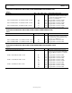
PD, SYNC, AND RESET PINS
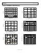
Table 15.
Parameter Min Typ Max Unit Test Conditions/Comments
INPUT CHARACTERISTICS
These pins each have a 30 kΩ internal pull-up
resistor
Logic 1 Voltage 2.0 V
Logic 0 Voltage 0.8 V
Logic 1 Current 1 µA
Logic 0 Current 110 µA
Capacitance
2
pF
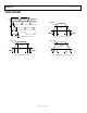
RESET TIMING
Pulse Width Low 50 ns
SYNC TIMING
Pulse Width Low 1.5
High speed
clock cycles
High speed clock is CLK input signal
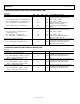
LD, STATUS, AND REFMON PINS
Table 16.
Parameter Min Typ Max Unit Test Conditions/Comments
OUTPUT CHARACTERISTICS
When selected as a digital output (CMOS);
there are other modes in which these pins
are not CMOS digital outputs; see Table 54,
Register 0x017, Register 0x01A, and
Register 0x01B
Output Voltage High (V
OH
) 2.7 V
Output Voltage Low (V
OL
) 0.4 V
MAXIMUM TOGGLE RATE 100 MHz
Applies when mux is set to any divider or
counter output, or PFD up/down pulse; also
applies in analog lock detect mode; usually
debug mode only; beware that spurs may
couple to output when any of these pins are
toggling
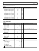
ANALOG LOCK DETECT
Capacitance 3 pF
On-chip capacitance; used to calculate RC
time constant for analog lock detect
readback; use a pull-up resistor
REF1, REF2, AND VCO FREQUENCY STATUS MONITOR
Normal Range 1.02 MHz
Frequency above which the monitor always
indicates the presence of the reference
Extended Range (REF1 and REF2 Only) 8 kHz
Frequency above which the monitor always
indicates the presence of the reference
LD PIN COMPARATOR
Trip Point 1.6 V
Hysteresis
260
mV