
Datasheet


AD9246
Rev. A | Page 9 of 44
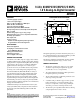
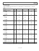
PIN CONFIGURATION AND FUNCTION DESCRIPTIONS
13
14
15
16
17
18
19
20
21
22
23
24
D12
D13 (MSB)
OR
DRGND
DRVDD
SDIO/DCS
SCLK/DFS
CSB
AGND
AVDD
AGND
AVDD
48
47
46
45
44
43
42
41
40
39
38
37
DRVDD
DRGND
D1
D0 (LSB)
DCO
OEB
AVDD
AGND
AVDD
CLK–
CLK+
AGND
1
2
3
4
5
6
7
8
9
10
11
12
D2
D3
D4
D5
D6
D7
DRGND
DRVDD
D8
D9
D10
D11
RBIAS
CML
AVDD
AGND
VIN–
VIN+
AGND
REFT
REFB
VREF
SENSE
35
PDWN36
34
33
32
31
30
29
28
27
26
25
AD9246
TOP VIEW
(Not to Scale)
PIN 1
INDICATOR
05491-003
Figure 3. Pin Configuration
Table 7. Pin Function Description
Pin No. Mnemonic Description
0, 21, 23, 29, 32,
37, 41
AGND Analog Ground. (Pin 0 is the exposed thermal pad on the bottom of the package.)
45, 46, 1 to 6,
9 to 14
D0 (LSB) to D13 (MSB) Data Output Bits.
7, 16, 47 DRGND Digital Output Ground.
8, 17, 48 DRVDD Digital Output Driver Supply (1.8 V to 3.3 V).
15 OR Out-of-Range Indicator.
18 SDIO/DCS
Serial Port Interface (SPI)® Data Input/Output (Serial Port Mode); Duty Cycle Stabilizer Select
(External Pin Mode). See
Table 10.
19 SCLK/DFS Serial Port Interface Clock (Serial Port Mode); Data Format Select Pin (External Pin Mode).
20 CSB Serial Port Interface Chip Select (Active Low). See Table 10.
22, 24, 33, 40, 42 AVDD Analog Power Supply.
25 SENSE Reference Mode Selection. See Table 9.
26 VREF Voltage Reference Input/Output.
27 REFB Differential Reference (−).
28 REFT Differential Reference (+).
30 VIN+ Analog Input Pin (+).
31 VIN– Analog Input Pin (−).
34 CML Common-Mode Level Bias Output.
35 RBIAS
External Bias Resistor Connection. A 10 kΩ resistor must be connected between this pin and
analog ground (AGND).
36 PDWN Power-Down Function Select.
38 CLK+ Clock Input (+).
39 CLK– Clock Input (−).
43 OEB Output Enable (Active Low).
44 DCO Data Clock Output.