
Datasheet


AD9246
Rev. A | Page 4 of 44
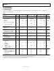
SPECIFICATIONS
DC SPECIFICATIONS
AVDD = 1.8 V; DRVDD = 2.5 V, maximum sample rate, 2 V p-p differential input, 1.0 V internal reference; AIN = −1.0 dBFS, DCS
enabled, unless otherwise noted.
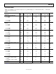
Table 1.
AD9246BCPZ-80 AD9246BCPZ-105 AD9246BCPZ-125
Parameter Temp
Min Typ Max Min Typ Max Min Typ Max Unit
RESOLUTION Full 14 14 14 Bits
ACCURACY
No Missing Codes Full Guaranteed Guaranteed Guaranteed
Offset Error Full ±0.3 ±0.5 ±0.3 ±0.8 ±0.3 ±0.8 % FSR
Gain Error Full ±0.6 ±4.7 ±0.6 ±5.0 ±0.6 ±4.2 % FSR
Differential Nonlinearity (DNL)
1
Full ±1.0 ±1.0 ±1.0 LSB
25°C ±0.4 ±0.4 ±0.4 LSB
Integral Nonlinearity (INL)
1
Full ±5.0 ±5.0 ±5.0 LSB
25°C ±1.5 ±1.3 ±1.5 LSB
TEMPERATURE DRIFT
Offset Error Full ±15 ±15 ±15 ppm/°C
Gain Error Full ±95 ±95 ±95 ppm/°C
INTERNAL VOLTAGE REFERENCE
Output Voltage Error (1 V Mode) Full ±5 ±20 ±5 ±35 ±5 ±35 mV
Load Regulation @ 1.0 mA Full 7 7 7 mV
INPUT REFERRED NOISE
VREF = 1.0 V 25°C 1.3 1.3 1.3 LSB rms
ANALOG INPUT
Input Span, VREF = 1.0 V Full
2 2
2 V p-p
Input Capacitance
2
Full
8 8
8 pF
REFERENCE INPUT RESISTANCE Full
6 6
6 kΩ
POWER SUPPLIES
Supply Voltage
AVDD Full
1.7 1.8 1.9 1.7 1.8 1.9
1.7 1.8 1.9 V
DRVDD Full
1.7 2.5 3.6 1.7 2.5 3.6
1.7 2.5 3.6 V
Supply Current
IAVDD
1
Full
138 155 178 194
220 236 mA
IDRVDD
1
(DRVDD = 1.8 V) Full
7 9
11 mA
IDRVDD
1
(DRVDD = 3.3 V) Full
12 16
19 mA
POWER CONSUMPTION
DC Input Full
248 279 320 350
395 425 mW
Sine Wave Input
1
(DRVDD = 1.8 V) Full
261 337
415 mW
Sine Wave Input
1
(DRVDD = 3.3 V) Full
288 373
458 mW
Standby Power
3
Full
40 40
40 mW
Power-Down Power Full
1.8 1.8
1.8 mW
1
Measured with a low input frequency, full-scale sine wave, with approximately 5 pF loading on each output bit.
2
Input capacitance refers to the effective capacitance between one differential input pin and AGND. Refer to Figure 4 for the equivalent analog input structure.
3
Standby power is measured with a dc input, the CLK pin inactive (set to AVDD or AGND).