
Datasheet


AD9246
Rev. A | Page 26 of 44
Addr.
(Hex)
Parameter Name
Bit 7
(MSB)
Bit 6 Bit 5 Bit 4 Bit 3 Bit 2 Bit 1
Bit 0
(LSB)
Default
Value
(Hex)
Default Notes/
Comments
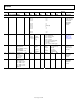
Flexible ADC Functions
10 offset
Digital Offset Adjust<5:0>
011111
011110
011101
…
000010
000001
000000
111111
111110
111101
...
100001
100000
Offset in LSBs
+31
+30
+29
+2
+1
0 (Default)
1
−2
−3
−31
−32
0x00 Adjustable for
offset inherent
in the converter.
See the
SPI-
Accessible
Features
section.
0D test_io PN23
0 =
normal
(Default)
1 = reset
PN9
0 =
normal
(Default)
1 =
reset
Global Output Test Options
000—off (Default)
001—midscale short
010—+FS short
011—−FS short
100—checker board output
101—PN 23 sequence
110—PN 9
111—one/zero word toggle
0x00 See the
Interfacing to
High Speed
ADCs via SPI
User Manual
.
14 output_mode Output Driver
Configuration
00 for DRVDD = 2.5 V to
3.3 V (Default)
10 for DRVDD = 1.8 V
Open Output
Disable
1—
disabled
0—
enabled
1
Open Output
Data
Invert
1 =
invert
Data Format Select
00—offset binary
(default)
01—twos
complement
10—Gray Code
0x00 Configures the
outputs and
the format of
the data.
16 output_phase
Output Clock
Polarity
1 = inverted
0 = normal
(Default)
Open Open Open Open Open Open Open 0x00
See the
SPI-
Accessible
Features
section.
18 VREF Internal Reference
Resistor Divider
00—VREF = 1.25 V
01—VREF = 1.5 V
10—VREF = 1.75 V
11—VREF = 2.00 V
(Default)
Open Open Open Open Open Open 0xC0
See the
SPI-
Accessible
Features
section.
1
External output enable (OEB) pin must be high.