
Datasheet


AD9246
Rev. A | Page 25 of 44
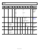
MEMORY MAP REGISTER TABLE
Table 15. Memory Map Register
Addr.
(Hex)
Parameter Name
Bit 7
(MSB)
Bit 6 Bit 5 Bit 4 Bit 3 Bit 2 Bit 1
Bit 0
(LSB)
Default
Value
(Hex)
Default Notes/
Comments
Chip Configuration Registers
00 chip_port_config 0 LSB first
0 = Off
(Default)
1 = On
Soft reset
0 = Off
(Default)
1 = On
1 1 Soft reset
0 = Off
(Default)
1 = On
LSB first
0 = Off
(Default)
1 = On
0 0x18 The nibbles
should be
mirrored. See the
Interfacing to
High Speed ADCs
via SPI User
Manual
.
01 chip_id 8-bit Chip ID Bits 7:0
(AD9246 = 0x00), (default)
Read
only
Default is unique
chip ID, different
for each device.
02 chip_grade Open Open Open Open Child ID
0 = 125
MSPS,
1 = 105
MSPS
Open Open Open Read
only
Child ID used to
differentiate
speed grades.
Device Index and Transfer Registers
FF device_update Open Open Open Open Open Open Open SW transfer 0x00 Synchronously
transfers data
from the master
shift register to
the slave.
Global ADC Functions
08 modes Open Open PDWN
0—full
(Default)
1—standby
Open Open Internal power-down mode
000—normal (power-up, Default)
001—full power-down
010—standby
011—normal (power-up)
Note: External PDWN pin overrides
this setting.
0x00 Determines
various generic
modes of chip
operation. See
the
Power
Dissipation
and Standby
Mode
section
and the
SPI-
Accessible
Features
section.
09 clock Open Open Open Open Open Open Open Duty cycle
stabilizer
0—disabled
1— enabled
(Default)
0x01
See the
Clock
Duty Cycle
section and the
SPI-Accessible
Features
section.