
Datasheet


AD9246
Rev. A | Page 22 of 44
TIMING
The lowest typical conversion rate of the AD9246 is 10 MSPS.
At clock rates below 10 MSPS, dynamic performance can degrade.
The AD9246 provides latched data outputs with a pipeline delay
of 12 clock cycles. Data outputs are available one propagation
delay (t
PD
) after the rising edge of the clock signal.
The length of the output data lines and the loads placed on
them should be minimized to reduce transients within the
AD9246. These transients can degrade the dynamic performance
of the converter.
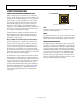
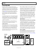
Data Clock Output (DCO)
The AD9246 provides a data clock output (DCO) intended for
capturing the data in an external register. The data outputs are valid
on the rising edge of DCO, unless the DCO clock polarity has
been changed via the SPI. See
Figure 2 for a graphical timing
description.
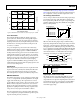
Table 12. Output Data Format
Input (V) Condition (V) Binary Output Mode Twos Complement Mode
Gray Code Mode
(SPI accessible)
OR
VIN+ – VIN– < –VREF – 0.5 LSB 00 0000 0000 0000 10 0000 0000 0000 11 0000 0000 0000 1
VIN+ – VIN– = –VREF 00 0000 0000 0000 10 0000 0000 0000 11 0000 0000 0000 0
VIN+ – VIN– = 0 10 0000 0000 0000 00 0000 0000 0000 00 0000 0000 0000 0
VIN+ – VIN– = +VREF – 1.0 LSB 11 1111 1111 1111 01 1111 1111 1111 10 0000 0000 0000 0
VIN+ – VIN– > +VREF – 0.5 LSB 11 1111 1111 1111 01 1111 1111 1111 10 0000 0000 0000 1