
Datasheet


AD9246
Rev. A | Page 20 of 44
The DCS can be enabled or disabled by setting the SDIO/DCS
pin when operating in the external pin mode (see
Table 10), or
via the SPI, as described in
Table 13.
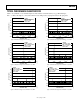
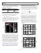
Table 10. Mode Selection (External Pin Mode)
Voltage at Pin SCLK/DFS SDIO/DCS
AGND Binary (default) DCS disabled
AVDD Twos complement
DCS enabled
(default)
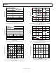
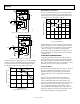
JITTER CONSIDERATIONS
High speed, high resolution ADCs are sensitive to the quality of
the clock input. The degradation in SNR at a given input
frequency (f
IN
) due to jitter (t
J
) is calculated as follows:
SNR = −20 log (2π × f
IN
× t
J
)
In the equation, the rms aperture jitter represents the root mean
square of all jitter sources, which include the clock input, analog
input signal, and ADC aperture jitter specification. IF under-
sampling applications are particularly sensitive to jitter, as
illustrated in
Figure 51.
75
70
65
60
55
50
45
40
1 10 100 1000
SNR (dBc)
INPUT FREQUENCY (MHz)
05491-083
3.00ps
0.05ps
MEASURED
PERFORMANCE
0.20ps
0.5ps
1.0ps
1.50ps
2.00ps
2.50ps
Figure 51. SNR vs. Input Frequency and Jitter
Treat the clock input as an analog signal in cases where aperture
jitter may affect the dynamic range of the AD9246. Power supplies
for clock drivers should be separated from the ADC output driver
supplies to avoid modulating the clock signal with digital noise.
The power supplies should also not be shared with analog input
circuits, such as buffers, to avoid the clock modulating onto the
input signal or vice versa. Low jitter, crystal-controlled oscillators
make the best clock sources. If the clock is generated from
another type of source (by gating, dividing, or other methods),
it should be retimed by the original clock at the last step.
Refer to Application Notes
AN-501, Aperture Uncertainty and
ADC System Performance, and
AN-756, Sampled Systems and
the Effects of Clock Phase Noise and Jitter, for more in-depth
information about jitter performance as it relates to ADCs.
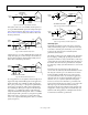
POWER DISSIPATION AND STANDBY MODE
As shown in Figure 52 and Figure 53, the power dissipated by
the AD9246 is proportional to its sample rate. The digital power
dissipation is determined primarily by the strength of the digital
drivers and the load on each output bit. The maximum DRVDD
current (I
DRVDD
) can be calculated as:
N
f
CVI
CLK
LOAD
DRVDDDRVDD
×××=
2
where N is the number of output bits, 14 in the case of the
AD9246.
This maximum current occurs when every output bit switches
on every clock cycle, that is, a full-scale square wave at the
Nyquist frequency, f
CLK
/2. In practice, the DRVDD current is
established by the average number of output bits switching,
which is determined by the sample rate and the characteristics
of the analog input signal. Reducing the capacitive load
presented to the output drivers can minimize digital power
consumption. The data in
Figure 52 and Figure 53 was taken
under the same operating conditions as the data for the
Typical
Performance Characteristics
section, with a 5 pF load on each
output driver.
475
325
01
CLOCK FREQUENCY (MSPS)
POWER (mW)
25
450
425
400
375
350
250
0
CURRENT (mA)
200
150
100
50
25 50 75 100
IDRVDD
IAVDD
TOTAL POWER
05491-034
Figure 52. AD9246-125 Power and Current vs. Clock Frequency f
IN
= 30 MHz
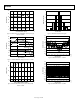
410
250
0
CLOCK FREQUENCY (MSPS)
POWER (mW)
200
180
0
CURRENT (mA)
160
140
120
100
80
60
40
20
25 50 75 100
390
370
350
330
310
290
270
IDRVDD
IAVDD
TOTAL POWER
05491-068
Figure 53. AD9246-105 Power and Current vs. Clock Frequency f
IN
= 30 MHz