
Datasheet


AD9246
Rev. A | Page 17 of 44
AD9246
R
0.1µF
0.1µF
2V p-p
VIN+
VIN–
CML
C
R
0.1µF
S
0.1µF
05491-080
25Ω
25Ω
SP
A
P
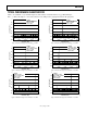
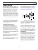
Figure 40. Differential Double Balun Input Configuration
AD9246
AD8352
0Ω
R
0Ω
C
D
R
D
R
G
0.1µF
0.1µF
0.1µF
VIN+
VIN–
CML
C
0.1µF
0.1µF
16
1
2
3
4
5
11
R
0.1µF
0.1µF
10
8, 13
14
V
CC
200Ω
200Ω
05491-081
A
NALOG INPUT
A
NALOG INPUT
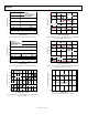
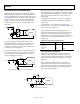
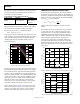
Figure 41. Differential Input Configuration Using the AD8352
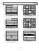
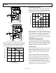
Table 9. Reference Configuration Summary
Selected Mode SENSE Voltage Resulting VREF (V)
Resulting Differential
Span (V p-p)
External Reference AVDD N/A 2 × External Reference
Internal Fixed Reference VREF 0.5 1.0
Programmable Reference 0.2 V to VREF
⎟
⎠
⎞
⎜
⎝
⎛
+×
R1
R2
15.0
(see Figure 43)
2 × VREF
Internal Fixed Reference AGND to 0.2 V 1.0 2.0
VOLTAGE REFERENCE
A stable and accurate voltage reference is built into the AD9246.
The input range is adjustable by varying the reference voltage
applied to the AD9246, using either the internal reference or an
externally applied reference voltage. The input span of the ADC
tracks reference voltage changes linearly. The various reference
modes are summarized in the following sections. The
Reference
Decoupling
section describes the best practices and require-
ments for PCB layout of the reference.
Internal Reference Connection
A comparator within the AD9246 detects the potential at the
SENSE pin and configures the reference into four possible
states, as summarized in
Table 9. If SENSE is grounded, the
reference amplifier switch is connected to the internal resistor
divider (see
Figure 42), setting VREF to 1 V.
Connecting the SENSE pin to VREF switches the reference
amplifier input to the SENSE pin, completing the loop and
providing a 0.5 V reference output.
If a resistor divider is connected external to the chip as shown
in
Figure 43, the switch sets to the SENSE pin. This puts the
reference amplifier in a noninverting mode with the VREF
output defined as
⎟
⎠
⎞
⎜
⎝
⎛
+=
R1
R2
VREF 15.0
If the SENSE pin is connected to AVDD, the reference amplifier
is disabled, and an external reference voltage can be applied to
the VREF pin (see the
External Reference Operation section).
The input range of the ADC always equals twice the voltage at
the reference pin for either an internal or an external reference.