
Datasheet


Data Sheet AD8479
Rev. 0 | Page 13 of 16
Typically, analog and digital grounds should be separated. At
the same time, however, the voltage difference between digital
and analog grounds on a converter must also be minimized to
keep this difference as small as possible (typically <0.3 V). The
increased noise—caused by the digital return currents of the
converter flowing through the analog ground plane—is typically
negligible.
Maximum isolation between analog and digital signals is
achieved by connecting the ground planes back to the supplies.
Note that Figure 36 suggests a star ground system for the analog
circuitry, with all ground lines connected, in this case, to the
analog ground of the ADC. However, when ground planes are
used, it is sufficient to connect ground pins to the nearest point
on the low impedance ground plane.
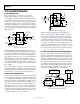
If only one power supply is available, it must be shared by both
digital and analog circuitry. Figure 37 shows how to minimize
interference between the digital and analog circuitry. In Figure 37,
the reference of the ADC is used to drive the REF(+) and REF(−)
pins of the AD8479. This means that the reference must be capable
of sourcing and sinking a current equal to V
CM
/500 kΩ.
POWER SUPPLY
V
IN1
V
IN2
V
DD
AGND DGND
ADC
0.1µF
0.1µF
+IN
–IN
+V
S
OUTPUT
–V
S
AD8479
REF(–) REF(+)
V
REF
47
3
2
6
1 5
V
DD
GND
MICROPROCESSOR
+5V
GND
0.1µF
11118-037
Figure 37. Optimal Grounding Practice for a Single-Supply Environment
As in the dual-supply environment, separate analog and digital
ground planes should be used (although reasonably thick traces
can be used as an alternative to a digital ground plane). These
ground planes should connect at the ground pin of the power
supply. Separate traces (or power planes) should run from the
power supply to the supply pins of the digital and analog circuits.
Ideally, each device should have its own power supply trace, but
these traces can be shared by a number of devices, as long as a
single trace is not used to route current to both digital and
analog circuitry.
USING A LARGE SHUNT RESISTOR
The insertion of a large value shunt resistor across the input pins,
Pin 2 and Pin 3, unbalances the input resistor network, thereby
introducing common-mode error. The magnitude of the error
depends on the common-mode voltage and the magnitude of
the shunt resistor (R
SHUNT
).
Table 4 shows some sample error voltages generated by a
common-mode voltage of 600 V dc with shunt resistors from
20 Ω to 2000 Ω. Assuming that the shunt resistor is selected to
use the full ±10 V output swing of the AD8479, the error voltage
becomes quite significant as the value of R
SHUNT
increases.
Table 4. Error Resulting from Large Values of R
SHUNT
(Uncompensated Circuit)
R
SHUNT
(Ω) Error V
OUT
(V) Error Indicated (mA)
20 0.012 0.6
1000 0.583 0.6
2000 1.164 0.6
To measure low current or current near zero in a high common-
mode voltage environment, an external resistor equal to the shunt
resistor value can be added to the low impedance side of the shunt
resistor, as shown in Figure 38.
REF(–)
REF(+)
–V
S
–V
S
+V
S
+V
S
V
OUT
NC
–IN
+IN
R
SHUNT
R
COMP
I
SHUNT
0.1µF
0.1µF
NC = NO CONNECT
AD8479
1
2
3
4
8
7
6
5
11118-038
Figure 38. Compensating for Large Shunt Resistors