
Datasheet


Data Sheet AD824
APPLICATIONS INFORMATION
SINGLE SUPPLY VOLTAGE-TO-FREQUENCY
CONVERTER
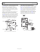
The circuit shown in Figure 32 uses the AD824 to drive a low
power timer, which produces a stable pulse of width, t
1
. The
positive going output pulse is integrated by R1 and C1 and used
as one input to the AD824, which is connected as a differential
integrator. The other input (nonloading) is the unknown
voltage, V
IN
. The AD824 output drives the timer trigger input,
closing the overall feedback loop.
1/4
AD824
U4
REF02
R
SCALE
**
10kΩ
2
6
5
4
3
V
REF
= 5V
CMOS
74HCO4
4 3 2 1
U3B U3A
OUT2
OUT1
10V
U1
2
6
5
3
7
1
4 8
U2
CMOS 555
TR
THR
DIS
CV
OUT
R V+
GND
0V TO 2.5V
FULL SCALE
C3
0.1µF
C4
0.1µF
C6
390pF
5%
(NPO)
R2
499kΩ
1%
R3*
116kΩ
C2
0.01µF
2%
C1
0.01µF
2%
C5
0.1µF
R1
499kΩ
1%
NOTES
f
OUT
= V
IN
/(V
REF
× t
1
), t
1
= 1.1 × R3 × C6 = 25kHz f
S
AS SHOWN.
* = 1% METAL FILM, <50ppm/°C TC
** = 10%, 20T FILM, <100ppm/°C TC
t
1
= 33µs FOR f
OUT
= 20kHz @ V
IN
= 2.0V
00875-032
Figure 32. Single Supply Voltage-to-Frequency Converter
Typical AD824 bias currents of 2 pA allow MΩ range source
impedances with negligible dc errors. Linearity errors of 0.01%
full scale can be achieved with this circuit. This performance is
obtained with a 5 V single supply, which delivers less than 3 mA
to the entire circuit.
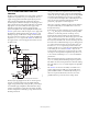
SINGLE SUPPLY PROGRAMMABLE GAIN
INSTRUMENTATION AMPLIFIER
The AD824 can be configured as a single supply instrumenta-
tion amplifier that is able to operate from single supplies down
to 5 V or dual supplies up to ±1 5 V. AD824 FET inputs bias
currents of 2 pA minimize offset errors caused by high
unbalanced source impedances.
An array of precision thin-film resistors sets the in amp gain to
be either 10 or 100. These resistors are laser-trimmed to ratio
match to 0.01% and have a maximum differential TC of
5 ppm/°C.
Table 6. AD824 In Amp Performance
Parameter V
S
= 3 V, 0 V V
S
= ±5 V
CMRR 74 dB 80 dB
Common-Mode Voltage Range
−0.2 V to +2 V
−5.2 V to +4 V
3 dB BW
G = 10 180 kHz 180 kHz
G = 100 18 kHz 18 kHz
t
SETTLING
2 V Step (V
S
= 0 V, 3 V) 2 μs
5 V (V
S
= ± 5 V) 5 μs
Noise @ f = 1 kHz
G = 10 270 nV/√Hz 270 nV/√Hz
G = 100 2.2 μV/√Hz 2.2 μV/√Hz
10
0%
100
90
1V
5µs
00875-033
Figure 33. Pulse Response of In Amp to a 500 mV p-p Input Signal;
V
S
= 5 V, 0 V; Gain = 10
V
OUT
+V
S
0.1µF
R6
90kΩ
R5
9kΩ
R4
1kΩ
R3
1kΩ
R2
9kΩ
R1
90kΩ
G = 10 G = 10G = 100G = 100
OHMTEK
PART #1043
2
1
3
6
7
5
11
1/4
AD824
1/4
AD824
V
REF
V
IN1
R
P
1kΩ
R
P
1kΩ
V
IN2
(G = 10) V
OUT
= (V
IN1
– V
IN2
)(1 + ) + V
REF
R6
R4 + R5
FOR R1 = R6, R2 = R5 AND R3 = R4
(G = 10) V
OUT
= (V
IN1
– V
IN2
)(1 + ) + V
REF
R5 + R6
R4
00875-034
Figure 34. A Single Supply Programmable Instrumentation Amplifier
Rev. E | Page 13 of 16