
Datasheet


Data Sheet AD8122
Rev. 0 | Page 5 of 20
ABSOLUTE MAXIMUM RATINGS
Table 2.
Parameter Rating
Supply Voltage 11 V
Power Dissipation
See Figure 2
Input Voltage (Any Input) V
S−
− 0.3 V to V
S+
+ 0.3 V
Storage Temperature Range −65°C to +125°C
Operating Temperature Range −40°C to +85°C
Lead Temperature (Soldering, 10 sec) 300°C
Junction Temperature 150°C
Stresses above those listed under Absolute Maximum Ratings
may cause permanent damage to the device. This is a stress
rating only; functional operation of the device at these or any
other conditions above those indicated in the operational
section of this specification is not implied. Exposure to absolute
maximum rating conditions for extended periods may affect
device reliability.
THERMAL RESISTANCE
θ
JA
is specified for the worst-case conditions, that is, the device
soldered in a circuit board in still air. This value was measured
using a JEDEC standard 4-layer printed circuit board (PCB).
Table 3. Thermal Resistance
Package Type θ
JA
θ
JC
Unit
40-Lead LFCSP 39 1.3 °C/W
MAXIMUM POWER DISSIPATION
The maximum safe power dissipation in the AD8122 package
is limited by the associated rise in junction temperature (T
J
) on
the die. At approximately 150°C, which is the glass transition
temperature, the plastic changes its properties. Even temporarily
exceeding this temperature limit can change the stresses that the
package exerts on the die, permanently shifting the parametric
performance of the AD8122. Exceeding a junction temperature
of 175°C for an extended period can result in changes in the
silicon devices, potentially causing failure.
The power dissipated in the package (P
D
) is the sum of the
quiescent power dissipation and the power dissipated in the
package due to the load drive for all outputs. The quiescent
power is the voltage between the supply pins (V
S+
and V
S−
)
times the quiescent current (I
S
). The power dissipation due to
each load current is calculated by multiplying the load current
by the voltage difference between the associated power supply
and the output voltage. The total power dissipation due to load
currents is then obtained by taking the sum of the individual
power dissipations. RMS output voltages must be used when
dealing with ac signals.
Airflow reduces θ
JA
. In addition, more metal directly in contact
with the package leads from metal traces, through holes, ground,
and power planes reduces θ
JA
. The exposed pad on the underside
of the package must be soldered to a pad on the PCB surface that
is thermally connected to a solid plane (usually the ground plane)
to achieve the specified θ
JA
.
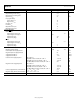
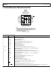
Figure 2 shows the maximum safe power dissipation in the
package vs. the ambient temperature for the 40-lead LFCSP
(θ
JA
= 39°C/W) on a JEDEC standard 4-layer board with the
exposed pad soldered to a pad that is thermally connected
to a PCB plane. θ
JA
values are approximations.
0
1
2
3
4
5
6
–40 –20 0 20 40 60 80
MAXIMUM POWER DISSIPATION (W)
AMBIENT TEMPERATURE (°C)
10780-003
Figure 2. Maximum Power Dissipation vs. Ambient Temperature
for a 4-Layer Board
ESD CAUTION