
Datasheet


AD8013
REV. A
–10–
4
+V
S
AD8013
1.0µF
0.1µF
11
1.0µF
0.1µF
–V
S
R
G
R
T
V
IN
15Ω
C
L
V
O
R
F
R
S
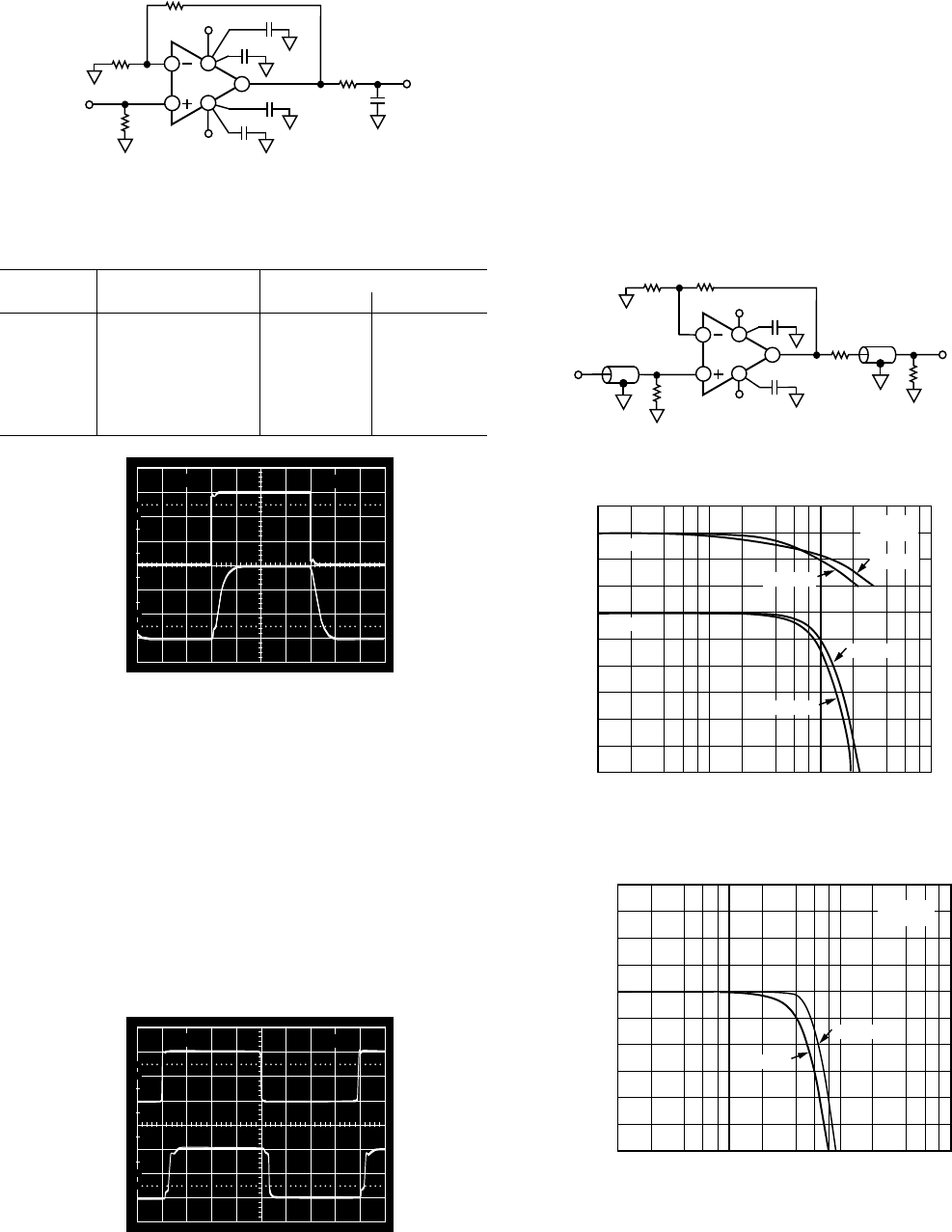
Figure 28. Circuit for Driving a Capacitive Load
Table II. Recommended Feedback and Series Resistors vs.
Capacitive Load and Gain
R
S
– Ohms
C
L
– pF R
F
– Ohms G = 2 G ≥ 3
20 2k 25 15
50 2k 25 15
100 3k 20 15
200 4k 15 15
300 6k 15 15
≥500 7k 15 15
10
0%
100
90
50ns
500mV
1V
V
IN
V
OUT
Figure 29. Pulse Response Driving a Large Load Capacitor.
C
L
= 300 pF, G = +2, R
F
= 6k, R
S
= 15
Ω
Overload Recovery
The three important overload conditions are: input common-
mode voltage overdrive, output voltage overdrive, and input
current overdrive. When configured for a low closed-loop gain,
the amplifier will quickly recover from an input common-
mode voltage overdrive; typically in under 25 ns. When con-
figured for a higher gain, and overloaded at the output, the
recovery time will also be short. For example, in a gain of +10,
with 15% overdrive, the recovery time of the AD8013 is about
20 ns (see Figure 30). For higher overdrive, the response is
somewhat slower. For 6 dB overdrive, (in a gain of +10), the
recovery time is about 65 ns.
10
0%
100
90
50ns
500mV
5V
V
IN
V
OUT
Figure 30. 15% Overload Recovery, G = +10 (R
F
= 300
Ω
,
R
L
= 1 k
Ω
, V
S
=
±
5 V)
As noted in the warning under “Maximum Power Dissipation,”
a high level of input overdrive in a high noninverting gain circuit
can result in a large current flow in the input stage. Though this
current is internally limited to about 30 mA, its effect on the
total power dissipation may be significant.
High Performance Video Line Driver
At a gain of +2, the AD8013 makes an excellent driver for a
back terminated 75 Ω video line (Figures 31, 32, and 33). Low
differential gain and phase errors and wide 0.1 dB bandwidth
can be realized. The low gain and group delay matching errors
ensure excellent performance in RGB systems. Figures 34 and
35 show the worst case matching.
75Ω
75Ω
V
OUT
75Ω
CABLE
75Ω
75Ω
CABLE
4
+V
S
AD8013
0.1µF
11
0.1µF
–V
S
R
G
V
IN
R
F
Figure 31. A Video Line Driver Operating at a Gain of +2
(R
F
= R
G
from Table I)
FREQUENCY – Hz
1M 1G10M
CLOSED-LOOP GAIN
(NORMALIZED) – dB
100M
–6
+1
0
–1
–2
–3
–4
–5
0
–90
–180
–270
PHASE SHIFT – Degrees
G = +2
R
L
= 150Ω
V
S
= ±5V
V
S
= +5V
V
S
= +5V
V
S
= ±5V
GAIN
PHASE
Figure 32. Closed-Loop Gain & Phase vs. Frequency
for the Line Driver
FREQUENCY – Hz
1M 1G10M
NORMALIZED GAIN – dB
100M
+0.1
0
–0.1
–0.2
–0.3
–0.4
–0.5
G = +2
R
L
= 150Ω
V
S
= +5V
V
S
= ±5V
+0.2
Figure 33. Fine-Scale Gain Flatness vs. Frequency,
G = +2, R
L
= 150
Ω