
Datasheet
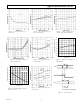

AD790
REV. B
–4–
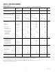
ABSOLUTE MAXIMUM RATINGS
1, 2
Supply Voltage . . . . . . . . . . . . . . . . . . . . . . . . . . . . . . . . ±18 V
Internal Power Dissipation
2
. . . . . . . . . . . . . . . . . . . 500 mW
Differential Input Voltage . . . . . . . . . . . . . . . . . . . . . ±16.5 V
Output Short Circuit Duration . . . . . . . . . . . . . . . . Indefinite
Storage Temperature Range
(N, R) . . . . . . . . . . . . . . . . . . . . . . . . . . . –65°C to +125°C
(Q) . . . . . . . . . . . . . . . . . . . . . . . . . . . . . . –65°C to +150°C
Lead Temperature Range (Soldering 60 sec) . . . . . . . +300°C
Logic Supply Voltage . . . . . . . . . . . . . . . . . . . . . . . . . . . . . 7 V
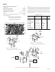
METALIZATION PHOTOGRAPH
Contact factory for latest dimensions.
Dimensions shown in inches and (mm).
Call factory for chip specifications.
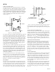
AD790
0.1µF
0.1µF
0.1µF
15V
+
+IN
–IN
5V
+
510
OUTPUT
15V
–
LATCH
(OPTIONAL)
8
1
5
7
6
4
3
2
Ω
Figure 1. Basic Dual Supply
Configuration (N, Q Package Pinout)
NOTES
1
Stresses above those listed under “Absolute Maximum Ratings” may cause
permanent damage to the device. This is a stress rating only and functional
operation of the device at these or any other conditions above those indicated in
the operational sections of this specification is not implied. Exposure to absolute
maximum rating conditions for extended periods may affect device reliability.
2
Thermal characteristics: plastic N-8 package: θ
JA
= 90°C/watt; ceramic Q-8
package: θ
JA
= 110°C/watt, θ
JC
= 30°C/watt. SOIC (R-8) package: θ
JA
= 160°C
watt; θ
JC
= 42°C/watt.
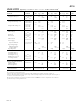
ORDERING GUIDE
Temperature Package Package
Model Range Description Option
AD790JN 0°C to +70°C Plastic DIP N-8
AD790JR 0°C to +70°C SOIC SO-8
AD790JR-REEL 0°C to +70°C Reel
AD790JR-REEL7 0°C to +70°C SOIC R-8
AD790KN 0°C to +70°C Plastic DIP N-8
AD790AQ –40°C to +85°C Cerdip Q-8
AD790BQ –40°C to +85°C Cerdip Q-8
AD790SQ –55°C to +125°C Cerdip Q-8
AD790SQ/883B –55°C to +125°C Cerdip Q-8
AD790S Chips –55°C to +125°C Die
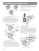
AD790
1
2
3
4
5
6
7
8
0.1µF
+IN
–IN
5V
+
OUTPUT
LATCH
(OPTIONAL)
510
Ω
Figure 2. Basic Single Supply
Configuration (N, Q Package Pinout)
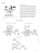
AD790
1
2
3
4
5
6
7
8
+5V
+15V
–15V
TEK
7904
SCOPE
–
5V
VOLTAGE
SOURCE
10Ω
–5mV
0.1µF
–100mV
–1.3V
–1.7V
–5V
HP8112
PULSE
GENERATOR
1k
HP2835
MPS
571
0.1µF
0.1µF
0.1µF
10kΩ
650Ω 400Ω 50Ω
25Ω
130Ω
Figure 3. Response Time Test Circuit (N, Q Package Pinout)