
Datasheet


Data Sheet AD7877
Rev. D | Page 43 of 44
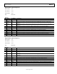
Register Name: GPIO Control Register 2
Write Address: [1111] 0001
Read Address: 11100
Default Value: 0x000
Type: Read/write
Table 23.
Bit Name Read/Write Description
0 GPIO4_ALEN R/W
If this bit is 1, GPIO4 is an interrupt source for the
ALERT output; clearing this bit masks out GPIO3
as an interrupt source for the ALERT output
1 GPIO4_DIR R/W This bit sets the direction of GPIO4
0 = output
1 = input
2 GPIO4_POL R/W This bit determines if GPIO4 is active high or low
0 = active low
1 = active high
3 Not Used This bit is not used
4 GPIO3_ALEN R/W
If this bit is 1, GPIO3 is an interrupt source for the
ALERT output; clearing this bit masks out GPIO4
as an interrupt source for the ALERT output
5 GPIO3_DIR R/W This bit sets the direction of GPIO3
0 = output
1 = input
6 GPIO3_POL R/W This bit determines if GPIO3 is active high or low
0 = active low
1 = active high
7 GPIO3_EN R/W This bit selects the function of AUX3/GPIO3
0 = AUX3
1 = GPIO3
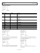
Register Name: GPIO Data Register
Write Address: [1111] 0010
Read Address: 11101
Default Value: 0x000
Type: Read/write
Table 24.
Bit Name Read/Write Description
0 Not used This bit is not used
1 Not used This bit is not used
2 Not used This bit is not used
3 Not used This bit is not used
4 GPIO4_DAT R/W GPIO4 data bit
5 GPIO3_DAT R/W GPIO3 data bit
6 GPIO2_DAT R/W GPIO2 data bit
7 GPIO1_DAT R/W GPIO1 data bit