
Datasheet


AD7877 Data Sheet
Rev. D | Page 40 of 44
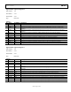
Register Name: DAC Register
Write Address: 1110
Read Address: 01110
Default Value: 0x008
Type: Read/write
Table 21.
Bit Name Read/Write Description
0 RANGE R/W Output range of the DAC in voltage mode
0 = 0 to V
CC
/2
1 = 0 to V
CC
1 Not Used R/W This bit is not used
2 V/I R/W Voltage output and current output
0 = voltage
1 = current
3 PD R/W DAC power-down
0 = DAC on
1 = DAC powered down
4 DAC0 LSB of DAC data
5 DAC1 Bit 1 of DAC data
6 DAC2 Bit 2 of DAC data
7 DAC3 Bit 3 of DAC data
8 DAC4 Bit 4 of DAC data
9 DAC5 Bit 5 of DAC data
10 DAC6 Bit 6 of DAC data
11 DAC7 MSB of DAC data
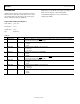
Register Name: Y Position
Write Address: N/A
Read Address: 10000
Default Value: 0x000
Type: Read only
This register contains the 12-bit result of the measurement at
the X+ input with Y layer excited (Y position measurement).
Register Name: X Position
Write Address: N/A
Read Address: 10001
Default Value: 0x000
Type: Read only
This register contains the 12-bit result of the measurement at
the Y+ input with X layer excited (X position measurement).
Register Name: Z2
Write Address: N/A
Read Address: 10010
Default Value: 0x000
Type: Read only
This register contains the 12-bit result of the measurement at
the Y− input with excitation voltage applied to Y+ and X− (used
for touch-pressure calculation).
Register Name: AUX1
Write Address: N/A
Read Address: 10011
Default Value: 0x000
Type: Read only
This register contains the 12-bit result of the measurement at
Auxiliary Input 1.