
Datasheet


AD7877 Data Sheet
Rev. D | Page 36 of 44
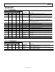
Register Name: Control Register 2
Write Address: 0010
Read Address: 00010
Default Value: 0x000
Type: Read/write
Table 17.
Bit Name Read/Write Description
0 TMR0 R/W LSB of conversion interval timer
1 TMR1 R/W MSB of conversion interval timer
00 = convert only once
01 = every 1024 clock periods (512 µs)
10 = every 2048 clock periods (1.024 ms)
11 = every 16,384 clock periods (8.19 ms)
2 REF R/W Selects internal or external reference
0 = internal reference
1 = external reference
3 POL R/W Indicates polarity of signal on STOPACQ pin
0 = active low
1 = active high
4 FCD0 R/W LSB of first conversion delay
5 FCD1 R/W MSB of first conversion delay
This delay occurs before the first conversion after powering up the ADC, before converting the X and Y
coordinate channels to allow settling, and after the last conversion to allow
PENIRQ precharge
00 = 1 clock period delay (500 ns)
01 = 256 clock periods delay (128 µs)
10 = 2048 clock periods delay (1.024 ms)
11 = 16,384 clock periods delay (8.19 ms)
6 PM0 R/W LSB of ADC power management code
7 PM1 R/W MSB of ADC power management code
00 = ADC and reference powered down continuously
For the following codes, regardless of PM bits, the reference is always powered down if the REF bit is 1:
01 = ADC and reference powered down when not converting
10 = ADC and reference powered up continuously (master sequencer does not work if PM = 10)
11 = ADC powered down when not converting, reference powered up
8 ACQ0 R/W LSB of ADC acquisition time
9 ACQ1 R/W MSB of ADC acquisition time
00 = 4 clock periods (2 µs)
01 = 8 clock periods (4 µs)
10 = 16 clock periods (8 µs)
11 = 32 clock periods (16 µs)
10 AVG0 R/W LSB of ADC averaging code
11 AVG1 R/W MSB of ADC averaging code
00 = no averaging (1 conversion per channel)
01 = 4 measurements per channel averaged
10 = 8 measurements per channel averaged
11 = 16 measurements per channel averaged