
Datasheet


Data Sheet AD7877
Rev. D | Page 33 of 44
REGISTER MAPS
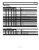
Table 13. Write Register Map
Register Address
Binary
WADD3 WADD2 WADD1 WADD0 Hex Register Name
Description
0 0 0 0 0 None Unused; writing to this address has no effect
0 0 0 1 1 Control Register 1
Contains ADC channel address, register read address, and ADC
mode
0
0
1
0
2
Control Register 2
Contains ADC averaging, acquisition time, power management,
first conversion delay, STOPACQ polarity, and reference and timer
settings
0
0
1
1
3
Alert
status/enable
register
Contains status of high/low limit comparisons for TEMP1, BAT1,
BAT2, and AUX1, and enable bits to allow these channels to
become interrupt sources
0
1
0
0
4
AUX1 high limit
User-programmable AUX1 upper limit
0 1 0 1 5 AUX1 low limit User-programmable AUX1 lower limit
0 1 1 0 6 BAT1 high limit User-programmable BAT1 upper limit
0
1
1
1
7
BAT1 low limit
User-programmable BAT1 lower limit
1 0 0 0 8 BAT2 high limit User-programmable BAT2 upper limit
1 0 0 1 9 BAT2 low limit User-programmable BAT2 lower limit
1 0 1 0 A TEMP1 low limit User-programmable TEMP1 lower limit
1 0 1 1 B TEMP1 high limit User-programmable TEMP1 upper limit
1 1 0 0 C
Sequencer
Register 0
Contains channel selection data for slave mode (software)
sequencing
1 1 0 1 D
Sequencer
Register 1
Contains channel selection data for master mode (hardware)
sequencing
1 1 1 0 E DAC register Contains DAC data and setup information
1 1 1 1 F Extended write Not a physical register; enables writing to extended writing map
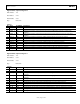
Table 14. Extended Writing Map
Register Address
Binary
EADD3
EADD2
EADD1
EADD0
Hex
Register Name
Description
0 0 0 0 0
GPIO Control
Register 1
Contains polarity, direction, enabling, and interrupt enabling
settings for GPIO1 and GPIO2
0 0 0 1 1
GPIO Control
Register 2
Contains polarity, direction, enabling, and interrupt enabling
settings for GPIO3 and GPIO4
0 0 1 0 2 GPIO data Contains GPIO1 to GPIO4 data