
Datasheet


AD7877 Data Sheet
Rev. D | Page 32 of 44
GROUNDING AND LAYOUT
It is recommended that the ground pins, AGND and DGND, be
shorted together as close as possible to the device itself on the
user’s PCB.
For more information on grounding and layout considerations
for the AD7877, refer to the AN-577 Application Note, Layout
and Grounding Recommendations for Touch Screen Digitizers.
PCB DESIGN GUIDELINES FOR CHIP SCALE
PACKAGES
The lands on the chip scale package (CP-32) are rectangular.
The printed circuit board pad for these should be 0.1 mm
longer than the package land length and 0.05 mm wider than
the package land width. To ensure that the solder joint size is
maximized, center the land on the pad.
The bottom of the chip scale package has a central thermal pad.
The thermal pad on the printed circuit board should be at least
as large as this exposed pad. On the printed circuit board, provide a
clearance of at least 0.25 mm between the thermal pad and the
inner edges of the pad pattern to ensure that shorting is avoided.
Using thermal vias on the printed circuit board thermal pad
improves the thermal performance of the package. If vias are
used, incorporate them in the thermal pad at a 1.2 mm pitch
grid. Keep the via diameter between 0.3 mm and 0.33 mm. The
via barrel should be plated with 1 oz. copper to plug the via.
The user should connect the printed circuit board thermal pad
to AGND.
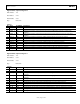
03796-026
HOST
NC = NO CONNECT
AD7877
24
NC
21
GPIO4
20
STOPACQ
19
DIN
17
PENIRQ
18
CS
22
ALERT
23
DAV
NC
1
BAT2
2
BAT1
3
AUX3/GPIO3
4
AUX2/GPIO2
5
AUX1/GPIO1
6
V
CC
7
NC
8
NC
32
V
REF
31
AOUT
30
ARNG
29
V
DRIVE
28
DOUT
27
DCLK
26
NC
25
NC
9
X–
10
Y–
11
X+
12
Y+
13
AGND
14
DGND
15
NC
16
INT1
SPI
INTERFACE
INT2
SCLK
MISO
MOSI
PENIRQ
CS
GPIO
HSYNC SIGNAL
FROM LCD
V
CC
R
RNG
0.1µF
DC-DC
CONVERTER
V
IN
OUT
FB
TO LCD
BACKLIGHT
TOUCH
SCREEN
0.1µF
1.0µF–10µF
(OPTIONAL)
VOLTAGE
REGULATOR
TEMPERATURE
MEASUREMENT
DIODE
MAIN
BATTERY
SECONDARY
BATTERY
FROM AUDIO
REMOTE CONTROL
FROM
HOTSYNC INPUTS
Figure 48. Typical Application Circuit