
Datasheet


Data Sheet AD7877
Rev. D | Page 21 of 44
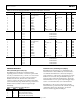
Table 6. Codes for Selecting Input Channel and Normal or Ratiometric Conversion
Channel
SER/
DFR
CHADD(3:0) Analog Input X Switches Y Switches +REF −REF
0 0 0 0 0 0 X+ (Y position) Off On Y+ Y−
1 0 0 0 0 1 Y+ (X position) On Off X+ X−
2 0 0 0 1 0 Y− (Z2) X+ off, X− on Y+ on, Y− off Y+ X−
3 0 0 01 1 AUX1 Off Off V
REF
GND
4 0 0 1 00 AUX2 Off Off V
REF
GND
5 0 0 1 0 1 AUX3 Off Off V
REF
GND
6 0 0 1 1 0 BAT1 Off Off V
REF
GND
7 0 0 1 1 1 BAT2 Off Off V
REF
GND
8 0 1 0 0 0 TEMP1 Off Off V
REF
GND
9
0
1 0 0 1
TEMP2
Off
Off
V
REF
GND
10 0 1 0 1 0 X+ (Z1) X+ OFF, X− ON Y+ on Y− off Y+ X−
- 0 1 0 1 1 Invalid address
-
0
1 1 0 0
Invalid address
- 0 1 1 0 1 Invalid address
- 0 1 1 1 0 Invalid address
- 0 1 1 1 1 Invalid address
0 1 0 0 0 0 X+ (Y position) Off On V
REF
GND
1 1 0 0 0 1 Y+ (X position) On Off V
REF
GND
2 1 0 0 1 0 Y− (Z2) X+ off, X− on Y+ on, Y− off V
REF
GND
3 1 0 0 1 1 AUX1 Off Off V
REF
GND
4
1
0 1 0 0
AUX2
Off
Off
V
REF
GND
5 1 0 1 0 1 AUX3 Off Off V
REF
GND
6 1 0 1 1 0 BAT1 Off Off V
REF
GND
7 1 0 1 1 1 BAT2 Off Off V
REF
GND
8 1 1 0 0 0 TEMP1 Off Off V
REF
GND
9 1 1 0 0 1 TEMP2 Off Off V
REF
GND
10
1
1 0 1 0
X+ (Z1)
X+ off, X− on
Y+ on, Y− off
V
REF
GND
- 1 10 1 1 Invalid address
- 1 1 1 0 0 Invalid address
-
1
1 1 0 1
Invalid address
- 1 1 1 1 0 Invalid address
- 1 1 1 1 1 Invalid address
CONTROL REGISTER 2
Timer (Control Register 2, Bits[1:0])
The TMR bits in Control Register 2 enable the ADC to
repeatedly perform a conversion or conversion sequence either
once only or at intervals of 512 µs, 1.024 ms, or 8.19 ms. In slave
mode, the timer starts as soon as the conversion sequence is
finished. In master mode, the timer starts at the end of a
conversion sequence only if the screen remains touched. If the
touch is released at any stage, then the timer stops and, the next
time the screen is touched, a conversion sequence begins
immediately.
Table 7. Control Register 2 Timer Selection
TMR1 TMR0 Function
0 0 Convert only once (default)
0 1 Every 1024 clocks (512 µs)
1 0 Every 2048 clocks (1.024 ms)
1 1 Every 16,384 clocks (8.19 ms)
Int/Ext Reference (Control Register 2, Bit[2])
If the REF bit in Control Register 2 is 0 (default value), the
internal reference is selected. Buffer any connection made to
V
REF
while the internal reference is selected (for example, to
supply a reference to other circuits). An external power supply
should not be connected to this pin while REF is equal to 0,
because it might overdrive the internal reference. Because the
internal reference is 2.5 V, it operates only with supply voltages
down to 2.7 V. Below this value, use an external reference.
If the REF bit is 1, the V
REF
pin becomes an input and the
internal reference is powered down. This overrides any setting
of the PM bits with regard to the reference. An external
reference can then be applied to the REF pin.