
Datasheet


Table Of Contents
- FEATURES
- GENERAL DESCRIPTION
- FUNCTIONAL BLOCK DIAGRAM
- PRODUCT HIGHLIGHTS
- SPECIFICATIONS
- Test Circuits
- ABSOLUTE MAXIMUM RATINGS
- PIN CONFIGURATIONS
- ORDERING GUIDE
- Typical Performance Characteristics
- OPERATIONAL DIAGRAM
- CIRCUIT INFORMATION BASIC DESCRIPTION
- APPLYING THE AD7824/AD7828 REFERENCE AND INPUT
- INPUT CURRENT
- INHERENT SAMPLE-HOLD
- SINUSOIDAL INPUTS
- UNIPOLAR OPERATION
- BIPOLAR OPERATION
- TIMING AND CONTROL
- MODE 0
- MODE 1
- MICROPROCESSOR INTERFACING
- Z80 MICROPROCESSOR
- MC68000 MICROPROCESSOR
- TMS32010 MICROCOMPUTER
- OUTLINE DIMENSIONS
- Revision History
AD7824/AD7828
REV. F
–9–
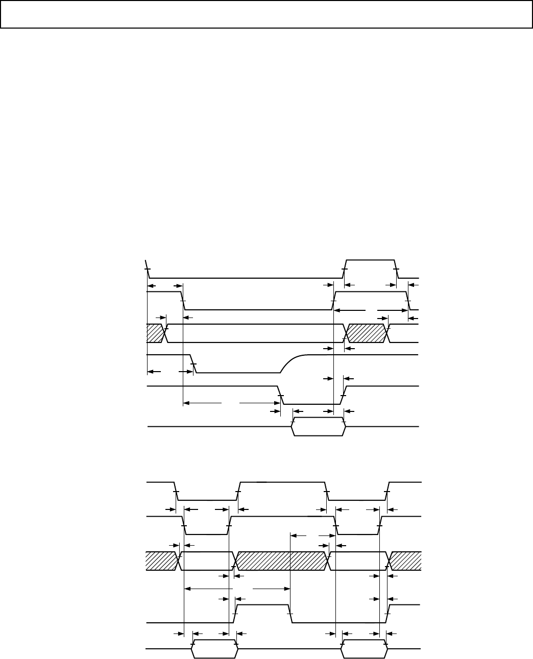
MODE 0
Figure 14 shows the timing diagram for Mode 0 operation. This
mode can only be used for microprocessors that have a WAIT
state facility, whereby a READ instruction cycle can be extended
to accommodate slow memory devices. A READ operation brings
CS and RD low, which starts a conversion. The analog multiplexer
address inputs must remain valid while CS and RD are low. The
data bus (DB7–DB0) remains in the three-state condition until
conversion is complete. There are two converter status outputs on
the AD7824/AD7828, interrupt (INT) and ready (RDY), which
can be used to drive the microprocessor READY/WAIT input.
The RDY is an open-drain output (no internal pull-up device) that
goes low on the falling edge of CS and goes high impedance at the
end of conversion when the 8-bit conversion result appears on the
data outputs. If the RDY status is not required, the external
pull-up resistor can be omitted and the RDY output tied to GND.
The INT goes low when conversion is complete and returns high
on the rising edge of CS or RD .
MODE 1
Mode 1 operation is designed for applications where the micropro-
cessor is not forced into a WAIT state. A READ operation takes
CS and RD low, which triggers a conversion (see Figure 15). The
multiplexer address inputs are latched on the rising edge of RD.
Data from the previous conversion is read from the three-state
data outputs (DB7–DB0). This data may be disregarded if not
required. Note that the RDY output (open drain output) does
not provide any status information in this mode and must be
connected to GND. At the end of conversion, INT goes low. A
second READ operation is required to access the new conversion
result. This READ operation latches a new address into the multi-
plexer inputs and starts another conversion. INT returns high at the
end of the second READ operation, when CS or RD returns high.
A delay of 2.5 µs must be allowed between READ operations.
CS
RD
ANALOG
CHANNEL
ADDRESS
RDY
INT
DATA
t
CSS
t
AS
t
RDY
t
CRD
t
ACC2
t
DH
t
INTH
t
AH
t
AS
t
P
t
CSS
t
CSH
ADDRESS
VA LI D
ADDRESS
VA LI D
DATA
VA LI D
HIGH IMPEDANCE
Figure 14. Mode 0 Timing Diagram
CS
RD
ANALOG
CHANNEL
ADDRESS
INT
DATA
t
CSS
t
AS
ADDRESS
VA LI D
OLD
VA LI D
ADDRESS
VA LI D
NEW
VA LI D
t
CSH
t
AH
t
RD
t
CRD
t
INTH
t
ACC1
t
DH
t
ACC1
t
DH
t
INTH
t
AH
t
AS
t
P
t
CSS
t
RD
t
CSH
Figure 15. Mode 1 Timing Diagram