
Datasheet


Data Sheet AD780
Rev. F | Page 9 of 12
00841-016
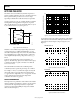
AD780
4
+V
IN
2
6
1µF
V
OUT
249Ω
V
L
V
OUT
0V
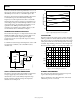
Figure 16. Transient Resistive Load Test Circuit
0mA
10mA
00841-017
10µs/DIV
OUTPUT CHANGE (50mV/DIV)
I
LOAD
V
OUT
(C
L
= 0pF)
Figure 17. Settling under Transient Resistive Load
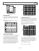
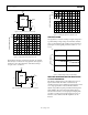
The dynamic load may be resistive and capacitive. For example,
the load may be connected via a long capacitive cable. Figure 18
and Figure 19 show the performance of the AD780 driving a
1000 pF, 0 mA to 10 mA load.
00841-018
AD780
4
+V
IN
2
6
1µ
F
V
OUT
249Ω
V
L
V
OUT
0V
C
L
1000pF
Figure 18. Capacitive Load Transient Response Test Circuit
0mA
10mA
00841-019
10µs/DIV
OUTPUT CHANGE (50mV/DIV)
I
LOAD
V
OUT
(C
L
= 1000pF)
Figure 19. Settling under Dynamic Capacitive Load
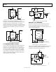
LINE REGULATION
Line regulation is a measure of change in output voltage due to
a specified change in input voltage. It is intended to simulate
worst-case unregulated supply conditions and is measured in
µV/V. Figure 20 shows typical performance with 4.0 V < V
IN
<
15.0 V.
200
100
0
–100
–200
4 1510
00841-020
INPUT VOLTAGE (V)
OUTPUT CHANGE (µ
V)
T = 25°
C
Figure 20. Output Voltage Change vs. Input Voltage
PRECISION REFERENCE FOR HIGH RESOLUTION
5 V DATA CONVERTERS
The AD780 is ideally suited to be the reference for most 5 V
high resolution ADCs. The AD780 is stable under any
capacitive load, has superior dynamic load performance, and its
3.0 V output provides the converter with the maximum
dynamic range without requiring an additional and expensive
buffer amplifier. One of the many ADCs that the AD780 is
suited for is the AD7884, a 16-bit, high speed sampling ADC
(see Figure 21). This part previously needed a precision 5 V
reference, resistor divider, and buffer amplifier to do this
function.