
Datasheet


–4–
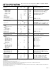
PIN FUNCTION DESCRIPTIONS
8-LEAD MSOP PIN NUMBERS*
Pin
No. Mnemonic Function
1 CLKOUT The crystal/resonator is tied between this pin and CLKIN. In the case of an external clock driving CLKIN, an
inverted clock signal appears on this pin and can be used to drive other circuitry provided it is buffered first.
2 CLKIN The master clock for the device may be in the form of a crystal/resonator tied between this pin and CLKOUT.
An external CMOS-compatible clock may also be applied to this input as the clock for the device. If CLKIN
is inactive low for 1 ms (typ), the AD7740 automatically enters power-down.
3 GND Ground reference for all the circuitry on-chip.
4 REFIN/OUT Voltage Reference Input. This is the reference input to the core of the VFC and defines the span of the VFC.
If this pin is left unconnected, the internal 2.5 V reference is the default reference. Alternatively, a precision
external reference may be used to overdrive the internal reference. The internal reference has high output
impedance in order to allow it to be overdriven.
5 VIN The analog input to the VFC. It has a nominal input range from 0 V to V
REF
which corresponds to an output
frequency of 10% f
CLKIN
to 90% f
CLKIN
. It has a ±150 mV overrange. If buffered, it draws virtually no current
from whatever source is driving it.
6 VDD Power Supply Input. These parts can be operated at 3.3 V ± 10% or 5 V ± 5%. The supply should be
adequately decoupled with a 10 µF and a 0.1 µF capacitor to GND.
7 FOUT Frequency Output. FOUT goes from 10% to 90% of f
CLKIN
, depending on VIN.
8 BUF Buffered Mode Select Pin. When BUF is tied low, the VIN input is unbuffered and the range on the VIN
pin is –0.15 V to VDD + 0.15 V. When it is tied high, VIN is buffered and the range on the VIN pin
is restricted to 0.1 V to VDD – 0.2 V.
*Note that the SOT-23 and MSOP packages have different pinouts.
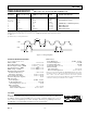
PIN CONFIGURATIONS
8-Lead MSOP
microSOIC
TOP VIEW
(Not to Scale)
8
7
6
5
1
2
3
4
CLKOUT
CLKIN
GND
REFIN/OUT
BUF
FOUT
VDD
VIN
AD7740
8-Lead SOT-23
SOT-23
TOP VIEW
(Not to Scale)
8
7
6
5
1
2
3
4
BUF
FOUT
VDD
VIN
CLKOUT
CLKIN
GND
REFIN/OUT
AD7740
REV. C
AD7740
ORDERING GUIDE
Model
1
Temperature Range Package Description Package Option Branding Information
8-Lead MSOP RM-8
V0K
8-Lead MSOP RM-8
V0K
8-Lead MSOP RM-8
V0K
0°C to +85°C
0°C to +85°C
0°C to +85°C
0°C to +85°C 8-Lead MSOP RM-8
V0K
8-Lead MSOP RM-8
V0Y
8-Lead MSOP RM-8
V0Y
8-Lead MSOP RM-8
V0Y
8-Lead MSOP RM-8
V0Y
AD7740KRM
AD7740KRMZ
AD7740KRMZ-REEL
AD7740KRMZ-REEL7
AD7740YRM
AD7740YRMZ
AD7740YRMZ-REEL
AD7740YRMZ-REEL7
AD7740YRTZ-REEL7
−40°C to +105°C
−40°C to +105°C
−40°C to +105°C
−40°C to +105°C
−40°C to +105°C 8-Lead SOT-23 RJ-8 C41
1
Z = RoHS Compliant Part.