
Datasheet


Data Sheet AD603
Rev. K | Page 7 of 24
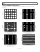
60
50
0
10
20
30
40
2 4 6 8 101214161820
PERCENTAGE OF SAMPLES (%)
OFFSET VOLTAGE (mV)
00539-057
553 PIECE SAMPLE SIZE
V
OS
AT 10dB GAIN
V
OS
VS V
GAIN
Figure 10. Histogram of V
OS
at 10 dB Gain and V
OS
vs. V
GAIN
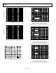
50
0
10
20
30
40
85 90 95 100 105 115110
PERCENTAGE OF SAMPLES (%)
PIN GPOS AND PIN GNEG BIAS CURRENT (nA)
00539-058
553 PIECE SAMPLE SIZE
GPOS
GNEG
Figure 11. Histogram of GPOS and GNEG Bias Current
00539-011
10dB/DIV
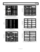
Figure 12. Third-Order Intermodulation Distortion at 455 kHz
(10× Probe Used to HP3585A Spectrum Analyzer, Gain = 0 dB, P
IN
= 0 dBm)
00539-012
10dB/DIV
Figure 13. Third-Order Intermodulation Distortion at 10.7 MHz
(10× Probe Used to HP3585A Spectrum Analyzer, Gain = 0 dB, P
IN
= 0 dBm)
00539-013
LOAD RESISTANCE (Ω)
0 50 100 200 500 1000 2000
NE
G
A
TIVE OUTPUT VOLTAGE (V)
–
1.0
–1.2
–1.4
–1.6
–1.8
–2.0
–2.2
–2.4
–2.6
–2.8
–3.0
–3.2
–3.4
Figure 14. Typical Output Voltage Swing vs. Load Resistance
(Negative Output Swing Limits First)
00539-014
FREQUENCY (Hz)
100M100k 1M 10M
INPUT IMPEDANCE
(
Ω)
102
100
98
94
96
Figure 15. Input Impedance vs. Frequency (Gain = −10 dB)