
Datasheet


Data Sheet AD603
Rev. K | Page 5 of 24
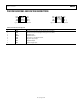
PIN CONFIGURATIONS AND FUNCTION DESCRIPTIONS
GPOS
1
GNEG
2
VINP
3
COMM
4
VPOS
8
VOUT
7
VNEG
6
FDBK
5
AD603
TOP VIEW
(Not to Scale)
00539-002
Figure 2. 8-Lead SOIC Pin Configuration
00539-003
GPOS
1
GNEG
2
VINP
3
COMM
4
VPOS
8
VOUT
7
VNEG
6
FDBK
5
AD603
TOP VIEW
(Not to Scale)
Figure 3. 8-Lead CERDIP Pin Configuration
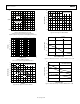
Table 4. Pin Function Descriptions
Pin No. Mnemonic Description
1 GPOS Gain Control Input High (Positive Voltage Increases Gain).
2 GNEG Gain Control Input Low (Negative Voltage Increases Gain).
3 VINP Amplifier Input.
4
COMM
Amplifier Ground.
5 FDBK Connection to Feedback Network.
6 VNEG Negative Supply Input.
7 VOUT Amplifier Output.
8 VPOS Positive Supply Input.