
Datasheet
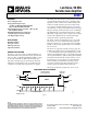


Data Sheet AD603
Rev. K | Page 3 of 24
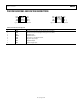
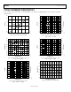
SPECIFICATIONS
@ T
A
= 25°C, V
S
= ±5 V, –500 mV ≤ V
G
≤ +500 mV, GNEG = 0 V, –10 dB to +30 dB gain range, R
L
= 500 Ω, and C
L
= 5 pF, unless
otherwise noted.
Table 1.
Parameter
Conditions
Min
Typ
Max
Unit
INPUT CHARACTERISTICS
Input Resistance
Pin 3 to Pin 4
97
100
103
Ω
Input Capacitance
2
pF
Input Noise Spectral Density
1
Input short-circuited
1.3
nV/√Hz
Noise Figure
f = 10 MHz, gain = maximum, R
S
= 10 Ω
8.8
dB
1 dB Compression Point
f = 10 MHz, gain = maximum, R
S
= 10 Ω
−11
dBm
Peak Input Voltage
±1.4
±2
V
OUTPUT CHARACTERISTICS
−3 dB Bandwidth
V
OUT
= 100 mV rms
90
MHz
Slew Rate
R
L
≥ 500 Ω
275
V/µs
Peak Output
2
R
L
≥ 500 Ω
±2.5
±3.0
V
Output Impedance
f ≤ 10 MHz
2
Ω
Output Short-Circuit Current
50
mA
Group Delay Change vs. Gain
f = 3 MHz; full gain range
±2
ns
Group Delay Change vs. Frequency
V
G
= 0 V; f = 1 MHz to 10 MHz
±2
ns
Differential Gain
0.2
%
Differential Phase
0.2
Degree
Total Harmonic Distortion
f = 10 MHz, V
OUT
= 1 V rms
−60
dBc
Third-Order Intercept
f = 40 MHz, gain = maximum, R
S
= 50 Ω
15
dBm
ACCURACY
Gain Accuracy, f = 100 kHz; Gain (dB) = (40 V
G
+ 10) dB
−500 mV ≤ V
G
≤ +500 mV
−1
±0.5
+1
dB
T
MIN
to T
MAX
−1.5
+1.5
dB
Gain, f = 10.7 MHz
V
G
= -0.5 V
−10.3
−9.0
−8.0
dB
V
G
= 0.0 V
+9.5
+10.5
+11.5
dB
V
G
= 0.5 V
+29.3
+30.3
+31.3
dB
Output Offset Voltage
3
V
G
= 0 V
20
mV
T
MIN
to T
MAX
30
mV
Output Offset Variation vs. V
G
−500 mV ≤ V
G
≤ +500 mV
20
mV
T
MIN
to T
MAX
30
mV
GAIN CONTROL INTERFACE
Gain Scaling Factor
100 kHz
39.4
40
40.6
dB/V
T
MIN
to T
MAX
38
42
dB/V
10.7 MHz
38.7
39.3
39.9
dB/V
GNEG, GPOS Voltage Range
4
−1.2
+2.0
V
Input Bias Current
50
100
250
nA
Input Offset Current
10
nA
Differential Input Resistance
Pin 1 to Pin 2
50
MΩ
Response Rate
Full 40 dB gain change
80
dB/µs
POWER SUPPLY
Specified Operating Range
±4.75
±6.3
V
Quiescent Current
12.5
17
mA
T
MIN
to T
MAX
20
mA
1
Typical open or short-circuited input; noise is lower when system is set to maximum gain and input is short-circuited. This figure includes the effects of both voltage
and current noise sources.
2
Using resistive loads of 500 Ω or greater or with the addition of a 1 kΩ pull-down resistor when driving lower loads.
3
The dc gain of the main amplifier in the AD603 is ×35.7; therefore, an input offset of 100 µV becomes a 3.57 mV output offset.
4
GNEG and GPOS, gain control, and voltage range are guaranteed to be within the range of −V
S
+ 4.2 V to +V
S
− 3.4 V over the full temperature range of −40°C to +85°C.