
Datasheet


AD603
Data Sheet
Rev. K | Page 20 of 24
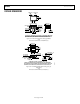
EVALUATION BOARD
The evaluation board of the AD603 enables simple bench-top
experimenting to be performed with easy control of the
AD603. Built-in flexibility allows convenient configuration to
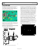
accommodate most operating configurations. Figure 50 is a
photograph of the AD603 evaluation board.
00539-049
Figure 50. AD603 Evaluation Board
Any dual-polarity power supply capable of providing 20 mA is
all that is required, in addition to whatever test equipment the
user wishes to perform the intended tests.
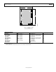
Referring to the schematic in Figure 51, the input to the VGA is
single-ended, ac-coupled, and terminated in 50 Ω to accommodate
most commonly available signal generators.
SCOM
G1 G2 G3 G4 G5 G6
+
+
GPOS
VINP VNEG
VOUT
VPOS
GNEG
COMM FDBK
VNEGVPOS GND
VNEGVPOS
VPOS
VPOS
R7
R1
GPOS
GPOSS
SGPOS
SGNEG
GNEG
VPOS
VNEG
VNEG
VNEG
R6
R5
GNEGS
VPOS
VIN
R8
R9
C2
0.1µF
C6
0.1µF
C3
0.1µF
R3
0Ω
C1
0.1µF
C4
0.1µF
C5
0.1µF
W2
4
3
2
1
5
6
7
8
R2
100Ω
AD603
R4
453Ω
W1
VO
VOUT
VNEG
C9
C7
10µF
25V
C8
10µF
25V
00539-050
Figure 51. Schematic of the AD603 Evaluation Board
The output is also ac-coupled and includes a 453 Ω series resistor.
Set the AD603 gain by connecting a voltage source between the
GNEG and GPOS test loops. The two slide switches SGPOS and
SGNEG provide three connections for GPOS and the GNEG.
Either pin can be ground referenced, or biased with a user selected
voltage established by R1 and R5 to R7. A signal generator can
be connected to the GPOS or GNEG test loops, or the GNEG can
be driven to either polarity within the common-mode limits of
−1.2 V to +2.0 V; to invert the gain slope, simply reverse the
polarity of the voltage source connected to GPOS and GNEG.
For bias current measurements, the third switch option
disconnects the bias voltage source and permits connection of a
microammeter between the GPOS and GNEG pins to ground.
The AD603 includes built-in gain resistors selectable at the
FDBK pin. The board is shipped with the gain at minimum,
with a 0 Ω resistor installed in R3. For maximum gain, simply
remove R3. Because of the architecture of the AD603, the
bandwidth decreases by 10, but the gain range remains at 40 dB.
Intermediate gain values may be selected by installing a resistor
between the VOUT and FDBK pins.
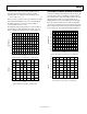
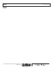
Figure 52, Figure 53, and Figure 56 show the component and
circuit side copper patterns and silkscreen.
00539-051
Figure 52. Component Side Copper