
Datasheet


Data Sheet AD603
Rev. K | Page 17 of 24
connected to the control voltage and the GNEW inputs are
grounded. The gain scaling is then doubled to 80 dB/V,
requiring only a 1.00 V change for an 80 dB change of gain
Gain = (dB) = 80 V
G
+ G
O
(4)
where, as before, G
O
depends on the range selected; for example,
in the maximum bandwidth mode, G
O
is 20 dB. Alternatively,
the GNEG pins may be connected to an offset voltage of
0.500 V, in which case G
O
is −20 dB.
The amplitude of the gain ripple in this case is also doubled, as
shown in Figure 45, while the ISNR at the output of A2 now
decreases linearly as the gain increases, as shown in Figure 46.
00539-043
V
C
(V)
2.2–0.2 0 0.2 0.4 0.6 1.0 1.20.8 1.6 1.8 2.01.4
GAIN ERROR (dB)
2.0
1.5
1.0
0.5
0
–0.5
–1.0
–1.5
–2.0
Figure 45. Gain Error for Cascaded Stages—Parallel Control
00539-044
V
C
(V)
1.2–0.2 0 0.2 0.4 0.6 0.8 1.0
ISNR (dB)
90
80
85
75
65
70
55
60
50
Figure 46. ISNR for Cascaded Stages—Parallel Control
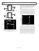
LOW GAIN RIPPLE MODE (MINIMUM GAIN ERROR)
As can be seen in Figure 44 and Figure 45, the error in the gain
is periodic, that is, it shows a small ripple. (Note that there is
also a variation in the output offset voltage, which is due to the
gain interpolation, but this is not exact in amplitude.) By
offsetting the gains of A1 and A2 by half the period of the ripple,
that is, by 3 dB, the residual gain errors of the two amplifiers
can be made to cancel. Figure 47 shows much lower gain ripple
when configured in this manner. Figure 48 plots the ISNR as a
function of gain; it is very similar to that in the parallel mode.
00539-045
V
C
(V)
1.1–0.1 0 0.1 0.2 0.3 0.4 0.5 0.6 0.7 0.8 0.9 1.0
GAIN ERROR (dB)
3.0
2.5
2.0
1.5
1.0
0.5
–0.5
–1.0
0
–1.5
–2.0
–2.5
–3.0
Figure 47. Gain Error for Cascaded Stages—Low Ripple Mode
00539-046
V
C
(V)
1.2–0.2 0 0.2 0.4 0.6 0.8 1.0
ISNR (dB)
90
85
80
75
70
65
60
55
50
Figure 48. ISNR vs. Control Voltage—Low Ripple Mode