
Datasheet


Table Of Contents
- Features
- Applications
- General Description
- Revision History
- Functional Block Diagram
- Specifications
- Absolute Maximum Ratings
- Pin Configuration and Function Descriptions
- Typical Performance Characteristics
- Terminology
- Theory of Operation
- Registers
- Design Features
- Applications Information
- Layout Guidelines
- Outline Dimensions
Data Sheet AD5764R
Rev. D | Page 21 of 32
THEORY OF OPERATION
The AD5764R is a quad, 16-bit, serial input, bipolar voltage output
DAC that operates from supply voltages of ±11.4 V to ±16.5 V and
has a buffered output voltage of up to ±10.5263 V. Data is written to
the AD5764R in a 24-bit word format via a 3-wire serial interface.
The AD5764R also offers an SDO pin that is available for daisy
chaining or readback.
The AD5764R incorporates a power-on reset circuit that ensures
that the data registers are loaded with 0x0000 at power-up. The
AD5764R features a digital I/O port that can be programmed via
the serial interface, an analog die temperature sensor, on-chip
10 ppm/°C voltage reference, on-chip reference buffers, and per
channel digital gain and offset registers.
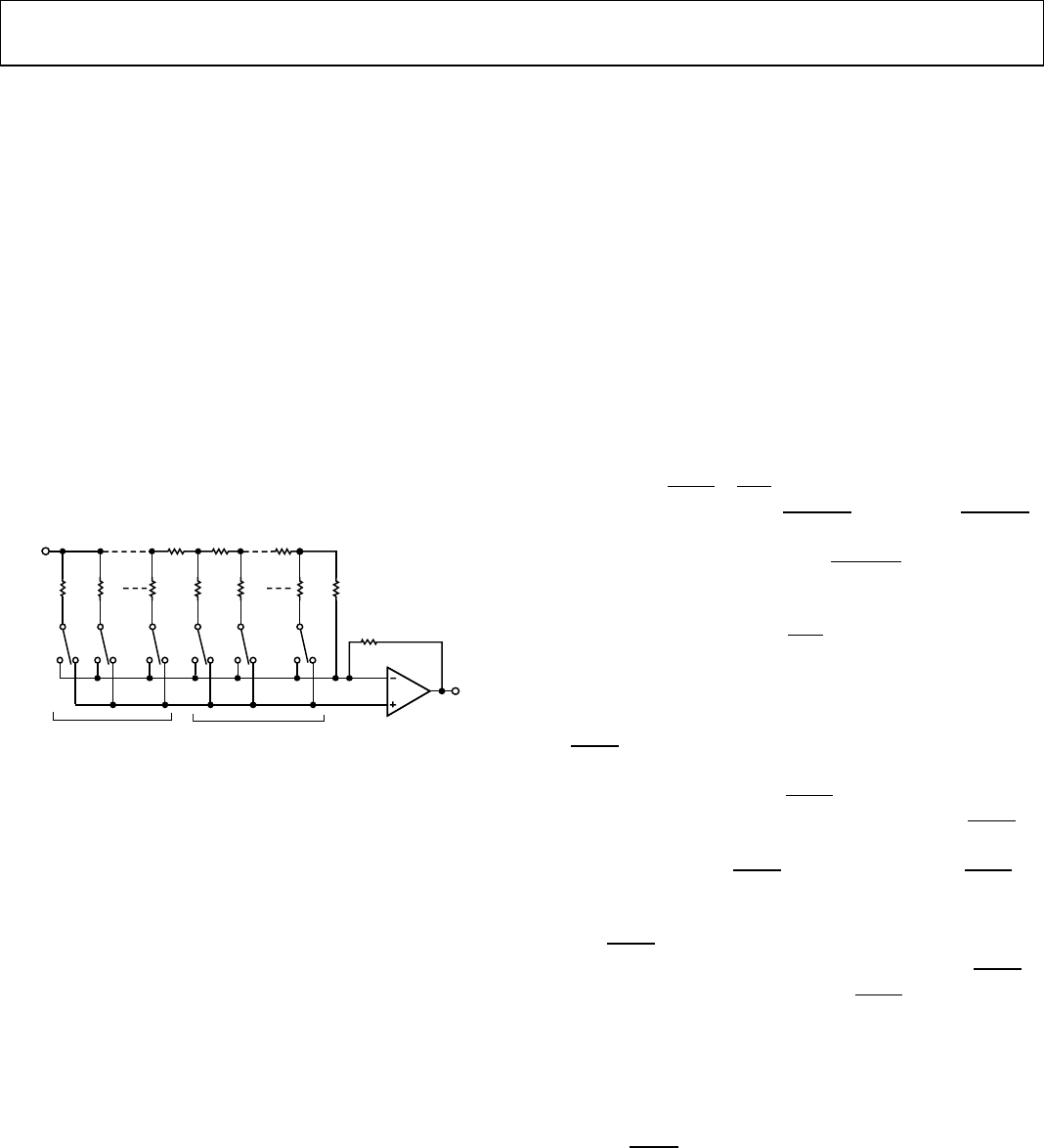
DAC ARCHITECTURE
The DAC architecture of the AD5764R consists of a 16-bit,
current mode, segmented R-2R DAC. The simplified circuit
diagram for the DAC section is shown in Figure 39.
06064-060
2R
E15
V
REF
2R
E14 E1
2R
S11
R R R
2R
S10
2R
12-BIT, R-2R LADDER4 MSBs DECODED INTO
15 EQUAL SEGMENTS
VOUTx
2R
S0
2R
AGNDx
R/8
I
OUT
Figure 39. DAC Ladder Structure
The four MSBs of the 16-bit data-word are decoded to drive
15 switches, E1 to E15. Each of these switches connects one
of the 15 matched resistors to either AGNDx or I
OUT
. The
remaining 12 bits of the data-word drive Switch S0 to Switch S11
of the 12-bit R-2R ladder network.
REFERENCE BUFFERS
The AD5764R can operate with either an external or an internal
reference. The reference inputs (REFAB and REFCD) have an
input range of up to 7 V. This input voltage is then used to provide
a buffered positive and negative reference for the DAC cores.
The positive reference is given by
+V
REF
= 2 × V
REFIN
The negative reference to the DAC cores is given by
−V
REF
= −2 × V
REFIN
These positive and negative reference voltages (along with the
gain register values) define the output ranges of the DACs.
SERIAL INTERFACE
The AD5764R is controlled over a versatile 3-wire serial interface
that operates at clock rates of up to 30 MHz and is compatible
with SPI, QSPI™, MICROWIRE™, and DSP standards.
Input Shift Register
The input shift register is 24 bits wide. Data is loaded into the
device, MSB first, as a 24-bit word under the control of a serial
clock input, SCLK. The input register consists of a read/write bit,
a reserved bit that must be set to 0, three register select bits, three
DAC address bits, and 16 data bits, as shown in Tabl e 9. The
timing diagram for this operation is shown in Figure 2.
Upon power-up, the data registers are loaded with zero code
(0x0000) and the outputs are clamped to 0 V via a low impedance
path. The outputs can be updated with the zero code value by
asserting either
LDAC
or
CLR
. The corresponding output voltage
depends on the state of the BIN/
2sCOMP
pin. If the BIN/
2sCOMP
pin is tied to DGND, the data coding is twos complement and
the outputs update to 0 V. If the BIN/
2sCOMP
pin is tied to
DV
CC
, the data coding is offset binary and the outputs update to
negative full scale. To have the outputs power up with zero code
loaded to the outputs, hold the
CLR
pin low during power-up.
Standalone Operation
The serial interface works with both a continuous and noncon-
tinuous serial clock. A continuous SCLK source can be used only
if
SYNC
is held low for the correct number of clock cycles. In
gated clock mode, a burst clock containing the exact number of
clock cycles must be used, and
SYNC
must be taken high after
the final clock to latch the data. The first falling edge of
SYNC
starts the write cycle. Exactly 24 falling clock edges must be
applied to SCLK before
SYNC
is brought high again. If
SYNC
is
brought high before the 24
th
falling SCLK edge, then the data
written is invalid. If more than 24 falling SCLK edges are applied
before
SYNC
is brought high, the input data is also invalid. The
input register addressed is updated on the rising edge of
SYNC
.
For another serial transfer to take place,
SYNC
must be brought
low again. After the end of the serial data transfer, data is
automatically transferred from the input shift register to the
addressed register.
When the data has been transferred into the chosen register of
the addressed DAC, all data registers and outputs can be updated
by taking
LDAC
low.