
User guide
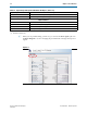
Table Of Contents
- Cyclone V Hard IP for PCI Express User Guide
- Contents
- 1. Datasheet
- 2. Getting Started with the Cyclone V Hard IP for PCI Express
- 3. Getting Started with the Avalon-MM Cyclone Hard IP for PCI Express
- Running Qsys
- Customizing the Cyclone VHard IP for PCI Express IP Core
- Adding the Remaining Components to the Qsys System
- Completing the Connections in Qsys
- Specifying Clocks and Interrupts
- Specifying Exported Interfaces
- Specifying Address Assignments
- Simulating the Example Design
- Simulating the Single DWord Design
- Understanding Channel Placement Guidelines
- Adding Synopsis Design Constraints
- Creating a Quartus II Project
- Compiling the Design
- Programming a Device
- 4. Parameter Settings for the Cyclone V Hard IP for PCI Express
- 5. Parameter Settings for the Avalon-MM Cyclone V Hard IP for PCI Express
- 6. IP Core Architecture
- Key Interfaces
- Protocol Layers
- Multi-Function Support
- PCI Express Avalon-MM Bridge
- Avalon-MM Bridge TLPs
- Avalon-MM-to-PCI Express Write Requests
- Avalon-MM-to-PCI Express Upstream Read Requests
- PCI Express-to-Avalon-MM Read Completions
- PCI Express-to-Avalon-MM Downstream Write Requests
- PCI Express-to-Avalon-MM Downstream Read Requests
- Avalon-MM-to-PCI Express Read Completions
- PCI Express-to-Avalon-MM Address Translation for Endpoints
- Minimizing BAR Sizes and the PCIe Address Space
- Avalon-MM-to-PCI Express Address Translation Algorithm
- Single DWord Completer Endpoint
- 7. IP Core Interfaces
- Cyclone V Hard IP for PCI Express
- Avalon-MM Hard IP for PCI Express
- Physical Layer Interface Signals
- Test Signals
- 8. Register Descriptions
- Configuration Space Register Content
- Altera-Defined Vendor Specific Extended Capability (VSEC)
- PCI Express Avalon-MM Bridge Control Register Access Content
- Avalon-MM to PCI Express Interrupt Registers
- PCI Express Mailbox Registers
- Avalon-MM-to-PCI Express Address Translation Table
- Root Port TLP Data Registers
- Programming Model for Avalon-MM Root Port
- PCI Express to Avalon-MM Interrupt Status and Enable Registers for Root Ports
- PCI Express to Avalon-MM Interrupt Status and Enable Registers for Endpoints
- Avalon-MM Mailbox Registers
- Correspondence between Configuration Space Registers and the PCIe Spec 2.1
- 9. Reset and Clocks
- 10. Transaction Layer Protocol (TLP) Details
- 11. Interrupts
- Interrupts for Endpoints Using the Avalon-ST Application Interface
- Interrupts for Root Ports Using the Avalon-ST Interface to the Application Layer
- Interrupts for Endpoints Using the Avalon-MM Interface to the Application Layer
- Interrupts for End Points Using the Avalon-MM Interface with Multiple MSI/MSI-X Support
- 12. Optional Features
- 13. Flow Control
- 14. Error Handling
- 15. Transceiver PHY IP Reconfiguration
- 16. SDC Timing Constraints
- 17. Testbench and Design Example
- Endpoint Testbench
- Root Port Testbench
- Chaining DMA Design Examples
- Test Driver Module
- Root Port Design Example
- Root Port BFM
- BFM Procedures and Functions
- 18. Debugging
- A. Transaction Layer Packet (TLP) Header Formats
- Additional Information

6–18 Chapter 6: IP Core Architecture
Avalon-MM Bridge TLPs
Cyclone V Hard IP for PCI Express December 2013 Altera Corporation
User Guide
2. System software programs BAR1:0 to have a base address of
0x00001234 56789000
3. A TLP received with address 0x00001234 56789870
4. The upper 52 bits (0x0000123456789) are used in the BAR matching process, so this
request matches.
5. The lower 12 bits, 0x870, are passed through as the Avalon address on the
Rxm_BAR0 Avalon-MM Master port. The BAR matching software replaces the
upper 20 bits of the address with the Avalon-MM base address.
Minimizing BAR Sizes and the PCIe Address Space
For designs that include multiple BARs, you may need to modify the base address
assignments auto-assigned by Qsys in order to minimize the address space that the
BARs consume. For example, consider a Qsys system with the following components:
■ Offchip_Data_Mem DDR3 (SDRAM Controller with UniPHY) controlling 256
MBytes of memory—Qsys auto-assigned a base address of 0x00000000
■ Quick_Data_Mem (On-Chip Memory (RAM or ROM)) of 4 KBytes—Qsys
auto-assigned a base address of 0x10000000
■ Instruction_Mem (On-Chip Memory (RAM or ROM)) of 64 KBytes—Qsys
auto-assigned a base address of 0x10020000
■ PCIe (Avalon-MM Cyclone V Hard IP for PCI Express)
■ Cra (Avalon-MM Slave)—auto assigned base address of 0x10004000
■ Rxm_BAR0 connects to Offchip_Data_Mem DDR3 avl
■ Rxm_BAR2 connects to Quick_Data_Mem s1
■ Rxm_BAR4 connects to PCIe. Cra Avalon-MM Slave
■ Nios2 (Nios
®
II Processor)
■ data_master connects to PCIe Cra, Offchip_Data_Mem DDR3 avl,
Quick_Data_Mem s1, Instruction_Mem s1, Nios2 jtag_debug_module
■ instruction_master connects to Instruction_Mem s1