
User guide
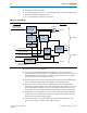
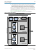
Table Of Contents
- Cyclone V Hard IP for PCI Express User Guide
- Contents
- 1. Datasheet
- 2. Getting Started with the Cyclone V Hard IP for PCI Express
- 3. Getting Started with the Avalon-MM Cyclone Hard IP for PCI Express
- Running Qsys
- Customizing the Cyclone VHard IP for PCI Express IP Core
- Adding the Remaining Components to the Qsys System
- Completing the Connections in Qsys
- Specifying Clocks and Interrupts
- Specifying Exported Interfaces
- Specifying Address Assignments
- Simulating the Example Design
- Simulating the Single DWord Design
- Understanding Channel Placement Guidelines
- Adding Synopsis Design Constraints
- Creating a Quartus II Project
- Compiling the Design
- Programming a Device
- 4. Parameter Settings for the Cyclone V Hard IP for PCI Express
- 5. Parameter Settings for the Avalon-MM Cyclone V Hard IP for PCI Express
- 6. IP Core Architecture
- Key Interfaces
- Protocol Layers
- Multi-Function Support
- PCI Express Avalon-MM Bridge
- Avalon-MM Bridge TLPs
- Avalon-MM-to-PCI Express Write Requests
- Avalon-MM-to-PCI Express Upstream Read Requests
- PCI Express-to-Avalon-MM Read Completions
- PCI Express-to-Avalon-MM Downstream Write Requests
- PCI Express-to-Avalon-MM Downstream Read Requests
- Avalon-MM-to-PCI Express Read Completions
- PCI Express-to-Avalon-MM Address Translation for Endpoints
- Minimizing BAR Sizes and the PCIe Address Space
- Avalon-MM-to-PCI Express Address Translation Algorithm
- Single DWord Completer Endpoint
- 7. IP Core Interfaces
- Cyclone V Hard IP for PCI Express
- Avalon-MM Hard IP for PCI Express
- Physical Layer Interface Signals
- Test Signals
- 8. Register Descriptions
- Configuration Space Register Content
- Altera-Defined Vendor Specific Extended Capability (VSEC)
- PCI Express Avalon-MM Bridge Control Register Access Content
- Avalon-MM to PCI Express Interrupt Registers
- PCI Express Mailbox Registers
- Avalon-MM-to-PCI Express Address Translation Table
- Root Port TLP Data Registers
- Programming Model for Avalon-MM Root Port
- PCI Express to Avalon-MM Interrupt Status and Enable Registers for Root Ports
- PCI Express to Avalon-MM Interrupt Status and Enable Registers for Endpoints
- Avalon-MM Mailbox Registers
- Correspondence between Configuration Space Registers and the PCIe Spec 2.1
- 9. Reset and Clocks
- 10. Transaction Layer Protocol (TLP) Details
- 11. Interrupts
- Interrupts for Endpoints Using the Avalon-ST Application Interface
- Interrupts for Root Ports Using the Avalon-ST Interface to the Application Layer
- Interrupts for Endpoints Using the Avalon-MM Interface to the Application Layer
- Interrupts for End Points Using the Avalon-MM Interface with Multiple MSI/MSI-X Support
- 12. Optional Features
- 13. Flow Control
- 14. Error Handling
- 15. Transceiver PHY IP Reconfiguration
- 16. SDC Timing Constraints
- 17. Testbench and Design Example
- Endpoint Testbench
- Root Port Testbench
- Chaining DMA Design Examples
- Test Driver Module
- Root Port Design Example
- Root Port BFM
- BFM Procedures and Functions
- 18. Debugging
- A. Transaction Layer Packet (TLP) Header Formats
- Additional Information

Chapter 6: IP Core Architecture 6–11
Protocol Layers
December 2013 Altera Corporation Cyclone V Hard IP for PCI Express
User Guide
■ LTSSM—This block implements the LTSSM and logic that tracks what is received
and transmitted on each lane.
■ For transmission, it interacts with each MAC lane sub-block and with the
LTSTX sub-block by asserting both global and per-lane control bits to generate
specific Physical Layer packets.
■ On the receive path, it receives the Physical Layer Packets reported by each
MAC lane sub-block. It also enables the multilane deskew block and the delay
required before the TX alignment sub-block can move to the recovery or low
power state. A higher layer can direct this block to move to the recovery,
disable, hot reset or low power states through a simple request/acknowledge
protocol. This block reports the Physical Layer status to higher layers.
■ LTSTX (Ordered Set and SKP Generation)—This sub-block generates the Physical
Layer Packet. It receives control signals from the LTSSM block and generates
Physical Layer Packet for each lane. It generates the same Physical Layer Packet
for all lanes and PAD symbols for the link or lane number in the corresponding
TS1/TS2 fields.
The block also handles the receiver detection operation to the PCS sub-layer by
asserting predefined PIPE signals and waiting for the result. It also generates a
SKP Ordered Set at every predefined timeslot and interacts with the TX alignment
block to prevent the insertion of a SKP Ordered Set in the middle of packet.
■ Deskew—This sub-block performs the multilane deskew function and the RX
alignment between the number of initialized lanes and the 64-bit data path.
The multilane deskew implements an eight-word FIFO for each lane to store
symbols. Each symbol includes eight data bits, one disparity bit, and one control
bit. The FIFO discards the FTS, COM, and SKP symbols and replaces PAD and
IDL with D0.0 data. When all eight FIFOs contain data, a read can occur.
When the multilane lane deskew block is first enabled, each FIFO begins writing
after the first COM is detected. If all lanes have not detected a COM symbol after
seven clock cycles, they are reset and the resynchronization process restarts, or
else the RX alignment function recreates a 64-bit data word which is sent to the
DLL.