
User guide
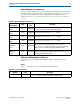
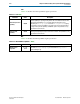

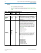
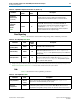

Table Of Contents
- Cyclone V Hard IP for PCI Express User Guide
- Contents
- 1. Datasheet
- 2. Getting Started with the Cyclone V Hard IP for PCI Express
- 3. Getting Started with the Avalon-MM Cyclone Hard IP for PCI Express
- Running Qsys
- Customizing the Cyclone VHard IP for PCI Express IP Core
- Adding the Remaining Components to the Qsys System
- Completing the Connections in Qsys
- Specifying Clocks and Interrupts
- Specifying Exported Interfaces
- Specifying Address Assignments
- Simulating the Example Design
- Simulating the Single DWord Design
- Understanding Channel Placement Guidelines
- Adding Synopsis Design Constraints
- Creating a Quartus II Project
- Compiling the Design
- Programming a Device
- 4. Parameter Settings for the Cyclone V Hard IP for PCI Express
- 5. Parameter Settings for the Avalon-MM Cyclone V Hard IP for PCI Express
- 6. IP Core Architecture
- Key Interfaces
- Protocol Layers
- Multi-Function Support
- PCI Express Avalon-MM Bridge
- Avalon-MM Bridge TLPs
- Avalon-MM-to-PCI Express Write Requests
- Avalon-MM-to-PCI Express Upstream Read Requests
- PCI Express-to-Avalon-MM Read Completions
- PCI Express-to-Avalon-MM Downstream Write Requests
- PCI Express-to-Avalon-MM Downstream Read Requests
- Avalon-MM-to-PCI Express Read Completions
- PCI Express-to-Avalon-MM Address Translation for Endpoints
- Minimizing BAR Sizes and the PCIe Address Space
- Avalon-MM-to-PCI Express Address Translation Algorithm
- Single DWord Completer Endpoint
- 7. IP Core Interfaces
- Cyclone V Hard IP for PCI Express
- Avalon-MM Hard IP for PCI Express
- Physical Layer Interface Signals
- Test Signals
- 8. Register Descriptions
- Configuration Space Register Content
- Altera-Defined Vendor Specific Extended Capability (VSEC)
- PCI Express Avalon-MM Bridge Control Register Access Content
- Avalon-MM to PCI Express Interrupt Registers
- PCI Express Mailbox Registers
- Avalon-MM-to-PCI Express Address Translation Table
- Root Port TLP Data Registers
- Programming Model for Avalon-MM Root Port
- PCI Express to Avalon-MM Interrupt Status and Enable Registers for Root Ports
- PCI Express to Avalon-MM Interrupt Status and Enable Registers for Endpoints
- Avalon-MM Mailbox Registers
- Correspondence between Configuration Space Registers and the PCIe Spec 2.1
- 9. Reset and Clocks
- 10. Transaction Layer Protocol (TLP) Details
- 11. Interrupts
- Interrupts for Endpoints Using the Avalon-ST Application Interface
- Interrupts for Root Ports Using the Avalon-ST Interface to the Application Layer
- Interrupts for Endpoints Using the Avalon-MM Interface to the Application Layer
- Interrupts for End Points Using the Avalon-MM Interface with Multiple MSI/MSI-X Support
- 12. Optional Features
- 13. Flow Control
- 14. Error Handling
- 15. Transceiver PHY IP Reconfiguration
- 16. SDC Timing Constraints
- 17. Testbench and Design Example
- Endpoint Testbench
- Root Port Testbench
- Chaining DMA Design Examples
- Test Driver Module
- Root Port Design Example
- Root Port BFM
- BFM Procedures and Functions
- 18. Debugging
- A. Transaction Layer Packet (TLP) Header Formats
- Additional Information

Chapter 4: Parameter Settings for the Cyclone V Hard IP for PCI Express 4–9
Port Functions
December 2013 Altera Corporation Cyclone V Hard IP for PCI Express
User Guide
Device ID Registers for Function <n>
Table 4–9 lists the default values of the read-only Device ID registers. You can use the
parameter editor to change the values of these registers. At run time, you can change
the values of these registers using the reconfiguration block signals. For more
information, refer to “R**Hard IP Reconfiguration Interface ###if_hip_reconfig###” on
page 8–52.
PCI Express/PCI Capabilities for Func <n>
The following sections describe the PCI Express and PCI Capabilities for each
function.
Device
Table 4–10 describes the Device Capabilities register parameters.
Table 4–9. Device ID Registers for Function <n>
Register Name/
Offset Address
Range
Default
Value
Description
Vendor ID
0x000
16 bits 0x00000000
Sets the read-only value of the
Vendor ID
register. This parameter can
not be set to 0xFFFF per the PCI Express Specification.
Device ID
0x000
16 bits 0x00000001 Sets the read-only value of the
Device ID
register.
Revision ID
0x008
8 bits 0x00000001 Sets the read-only value of the
Revision ID
register.
Class code
0x008
24 bits 0x00000000 Sets the read-only value of the
Class Code
register.
Subsystem
Vendor ID
0x02C
16 bits 0x00000000
Sets the read-only value of the
Subsystem Vendor ID
register. This
parameter cannot be set to 0xFFFF per the PCI Express Base
Specification 2.1. This register is available only for Endpoint designs
which require the use of the Type 0 PCI Configuration register.
Subsystem
Device ID
0x02C
16 bits 0x0000000
Sets the read-only value of the
Subsystem Device ID
register. This
register is only available for Endpoint designs, which require the use of
the Type 0 PCI Configuration Space.
Table 4–10. Function Level Reset
Parameter Value Description
Function level reset On/Off
Turn On this option to set the Function Level Reset Capability bit in the
Device
Capabilities
register. This parameter applies to Endpoints only.