
User guide

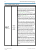
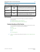
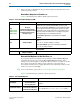
Table Of Contents
- Cyclone V Hard IP for PCI Express User Guide
- Contents
- 1. Datasheet
- 2. Getting Started with the Cyclone V Hard IP for PCI Express
- 3. Getting Started with the Avalon-MM Cyclone Hard IP for PCI Express
- Running Qsys
- Customizing the Cyclone VHard IP for PCI Express IP Core
- Adding the Remaining Components to the Qsys System
- Completing the Connections in Qsys
- Specifying Clocks and Interrupts
- Specifying Exported Interfaces
- Specifying Address Assignments
- Simulating the Example Design
- Simulating the Single DWord Design
- Understanding Channel Placement Guidelines
- Adding Synopsis Design Constraints
- Creating a Quartus II Project
- Compiling the Design
- Programming a Device
- 4. Parameter Settings for the Cyclone V Hard IP for PCI Express
- 5. Parameter Settings for the Avalon-MM Cyclone V Hard IP for PCI Express
- 6. IP Core Architecture
- Key Interfaces
- Protocol Layers
- Multi-Function Support
- PCI Express Avalon-MM Bridge
- Avalon-MM Bridge TLPs
- Avalon-MM-to-PCI Express Write Requests
- Avalon-MM-to-PCI Express Upstream Read Requests
- PCI Express-to-Avalon-MM Read Completions
- PCI Express-to-Avalon-MM Downstream Write Requests
- PCI Express-to-Avalon-MM Downstream Read Requests
- Avalon-MM-to-PCI Express Read Completions
- PCI Express-to-Avalon-MM Address Translation for Endpoints
- Minimizing BAR Sizes and the PCIe Address Space
- Avalon-MM-to-PCI Express Address Translation Algorithm
- Single DWord Completer Endpoint
- 7. IP Core Interfaces
- Cyclone V Hard IP for PCI Express
- Avalon-MM Hard IP for PCI Express
- Physical Layer Interface Signals
- Test Signals
- 8. Register Descriptions
- Configuration Space Register Content
- Altera-Defined Vendor Specific Extended Capability (VSEC)
- PCI Express Avalon-MM Bridge Control Register Access Content
- Avalon-MM to PCI Express Interrupt Registers
- PCI Express Mailbox Registers
- Avalon-MM-to-PCI Express Address Translation Table
- Root Port TLP Data Registers
- Programming Model for Avalon-MM Root Port
- PCI Express to Avalon-MM Interrupt Status and Enable Registers for Root Ports
- PCI Express to Avalon-MM Interrupt Status and Enable Registers for Endpoints
- Avalon-MM Mailbox Registers
- Correspondence between Configuration Space Registers and the PCIe Spec 2.1
- 9. Reset and Clocks
- 10. Transaction Layer Protocol (TLP) Details
- 11. Interrupts
- Interrupts for Endpoints Using the Avalon-ST Application Interface
- Interrupts for Root Ports Using the Avalon-ST Interface to the Application Layer
- Interrupts for Endpoints Using the Avalon-MM Interface to the Application Layer
- Interrupts for End Points Using the Avalon-MM Interface with Multiple MSI/MSI-X Support
- 12. Optional Features
- 13. Flow Control
- 14. Error Handling
- 15. Transceiver PHY IP Reconfiguration
- 16. SDC Timing Constraints
- 17. Testbench and Design Example
- Endpoint Testbench
- Root Port Testbench
- Chaining DMA Design Examples
- Test Driver Module
- Root Port Design Example
- Root Port BFM
- BFM Procedures and Functions
- 18. Debugging
- A. Transaction Layer Packet (TLP) Header Formats
- Additional Information

4–8 Chapter 4: Parameter Settings for the Cyclone V Hard IP for PCI Express
Port Functions
Cyclone V Hard IP for PCI Express December 2013 Altera Corporation
User Guide
1 When you click on a Func<n> tab, the parameter settings automatically relate to the
function currently selected.
Base Address Registers for Function <n>
Table 4–7 describes the Base Address (BAR) register parameters.
Base and Limit Registers for Root Port Func <n>
If you specify a Root Port for function 0, the settings for Base and Limit Registers
required by Root Ports appear after the Base Address Register heading. These
settings are stored in the Type 1 Configuration Space for Root Ports. They are used for
TLP routing and specify the address ranges assigned to components that are
downstream of the Root Port or bridge. Function 0 is the only function that provides
the Root Port option for Port type.
f For more information, refer to the PCI-to-PCI Bridge Architecture Specification.
Table 4–8 describes the Base and Limit
registers parameters.
Table 4–7. Func0–Func7 BARs and Expansion ROM
Parameter Value Description
Type
0x010, 0x014,
0x018, 0x01C,
0x020, 0x024
Disabled
64-bit prefetchable memory
32-bit non-prefetchable memory
32-bit prefetchable memory
I/O address space
If you select 64-bit prefetchable memory, 2 contiguous BARs are
combined to form a 64-bit prefetchable BAR; you must set the
higher numbered BAR to Disabled. A non-prefetchable 64-bit BAR
is not supported because in a typical system, the Root Port Type 1
Configuration Space sets the maximum non-prefetchable memory
window to 32-bits. The BARs can also be configured as separate
32-bit prefetchable or non-prefetchable memories.
The I/O address space BAR is only available for the Legacy
Endpoint.
Size 16 Bytes–8 EBytes
The Endpoint and Root Port variants support the following memory
sizes:
■ ×1, ×2, ×4: 128 bytes–2 GBytes or 8 EBytes
The Legacy Endpoint supports the following I/O space BARs:
■ ×1, ×2, ×4:16 bytes–4 KBytes
Expansion ROM
Size
Disabled
4 KBytes–16 MBytes
Specifies the size of the optional ROM.
Table 4–8. Base and Limit Registers
Parameter Value Description
Input/Output
Disable
16-bit I/O addressing
32-bit I/O addressing
Specifies the address widths for the
IO base
and
IO limit
registers.
Prefetchable memory
Disable
32-bit memory addressing
64-bit memory addressing
Specifies the address widths for the
Prefetchable Memory
Base
register and
Prefetchable Memory Limit
register.