
User guide

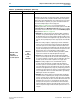
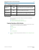
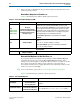
Table Of Contents
- Cyclone V Hard IP for PCI Express User Guide
- Contents
- 1. Datasheet
- 2. Getting Started with the Cyclone V Hard IP for PCI Express
- 3. Getting Started with the Avalon-MM Cyclone Hard IP for PCI Express
- Running Qsys
- Customizing the Cyclone VHard IP for PCI Express IP Core
- Adding the Remaining Components to the Qsys System
- Completing the Connections in Qsys
- Specifying Clocks and Interrupts
- Specifying Exported Interfaces
- Specifying Address Assignments
- Simulating the Example Design
- Simulating the Single DWord Design
- Understanding Channel Placement Guidelines
- Adding Synopsis Design Constraints
- Creating a Quartus II Project
- Compiling the Design
- Programming a Device
- 4. Parameter Settings for the Cyclone V Hard IP for PCI Express
- 5. Parameter Settings for the Avalon-MM Cyclone V Hard IP for PCI Express
- 6. IP Core Architecture
- Key Interfaces
- Protocol Layers
- Multi-Function Support
- PCI Express Avalon-MM Bridge
- Avalon-MM Bridge TLPs
- Avalon-MM-to-PCI Express Write Requests
- Avalon-MM-to-PCI Express Upstream Read Requests
- PCI Express-to-Avalon-MM Read Completions
- PCI Express-to-Avalon-MM Downstream Write Requests
- PCI Express-to-Avalon-MM Downstream Read Requests
- Avalon-MM-to-PCI Express Read Completions
- PCI Express-to-Avalon-MM Address Translation for Endpoints
- Minimizing BAR Sizes and the PCIe Address Space
- Avalon-MM-to-PCI Express Address Translation Algorithm
- Single DWord Completer Endpoint
- 7. IP Core Interfaces
- Cyclone V Hard IP for PCI Express
- Avalon-MM Hard IP for PCI Express
- Physical Layer Interface Signals
- Test Signals
- 8. Register Descriptions
- Configuration Space Register Content
- Altera-Defined Vendor Specific Extended Capability (VSEC)
- PCI Express Avalon-MM Bridge Control Register Access Content
- Avalon-MM to PCI Express Interrupt Registers
- PCI Express Mailbox Registers
- Avalon-MM-to-PCI Express Address Translation Table
- Root Port TLP Data Registers
- Programming Model for Avalon-MM Root Port
- PCI Express to Avalon-MM Interrupt Status and Enable Registers for Root Ports
- PCI Express to Avalon-MM Interrupt Status and Enable Registers for Endpoints
- Avalon-MM Mailbox Registers
- Correspondence between Configuration Space Registers and the PCIe Spec 2.1
- 9. Reset and Clocks
- 10. Transaction Layer Protocol (TLP) Details
- 11. Interrupts
- Interrupts for Endpoints Using the Avalon-ST Application Interface
- Interrupts for Root Ports Using the Avalon-ST Interface to the Application Layer
- Interrupts for Endpoints Using the Avalon-MM Interface to the Application Layer
- Interrupts for End Points Using the Avalon-MM Interface with Multiple MSI/MSI-X Support
- 12. Optional Features
- 13. Flow Control
- 14. Error Handling
- 15. Transceiver PHY IP Reconfiguration
- 16. SDC Timing Constraints
- 17. Testbench and Design Example
- Endpoint Testbench
- Root Port Testbench
- Chaining DMA Design Examples
- Test Driver Module
- Root Port Design Example
- Root Port BFM
- BFM Procedures and Functions
- 18. Debugging
- A. Transaction Layer Packet (TLP) Header Formats
- Additional Information

Chapter 4: Parameter Settings for the Cyclone V Hard IP for PCI Express 4–7
Port Functions
December 2013 Altera Corporation Cyclone V Hard IP for PCI Express
User Guide
Power Management
Table 4–6 describes the Power Management parameters.
Parameters Defined Separately for All Port Functions
You can specify parameter settings for up to eight functions. Each function has
separate settings for the following parameters:
■ Base Address Registers for Function <n>
■ Base and Limit Registers for Root Port Func <n>
■ Device ID Registers for Function <n>
■ PCI Express/PCI Capabilities for Func <n>
Slot power limit
0–255
In combination with the Slot power scale value, specifies the upper limit in watts on
power supplied by the slot. Refer to Section 7.8.9 of the
PCI Express Base Specification
Revision 2.1
for more information.
Slot number
0-8191
Specifies the slot number.
Table 4–5. Slot Capabilities 0x094
Parameter Value Description
Table 4–6. Power Management Parameters
Parameter Value Description
Endpoint L0s
acceptable latency
< 64 ns – > No limit
This design parameter specifies the maximum acceptable latency that the
device can tolerate to exit the L0s state for any links between the device and
the root complex. It sets the read-only value of the Endpoint L0s acceptable
latency field of the
Device Capabilities
register (0x084).
The Cyclone V Hard IP for PCI Express does not support the L0s or L1
states. However, in a switched system there may be links connected to
switches that have L0s and L1 enabled. This parameter is set to allow
system configuration software to read the acceptable latencies for all
devices in the system and the exit latencies for each link to determine which
links can enable Active State Power Management (ASPM). This setting is
disabled for Root Ports.
The default value of this parameter is 64 ns. This is the safest setting for
most designs.
Endpoint L1
acceptable latency
< 1 µs to > No limit
This value indicates the acceptable latency that an Endpoint can withstand
in the transition from the L1 to L0 state. It is an indirect measure of the
Endpoint’s internal buffering. It sets the read-only value of the Endpoint L1
acceptable latency field of the
Device Capabilities
register.
The Cyclone V Hard IP for PCI Express does not support the L0s or L1
states. However, in a switched system there may be links connected to
switches that have L0s and L1 enabled. This parameter is set to allow
system configuration software to read the acceptable latencies for all
devices in the system and the exit latencies for each link to determine which
links can enable Active State Power Management (ASPM). This setting is
disabled for Root Ports.
The default value of this parameter is 1 .µs. This is the safest setting for
most designs.