
User guide

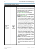
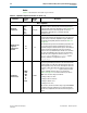
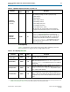
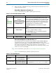
Table Of Contents
- Cyclone V Hard IP for PCI Express User Guide
- Contents
- 1. Datasheet
- 2. Getting Started with the Cyclone V Hard IP for PCI Express
- 3. Getting Started with the Avalon-MM Cyclone Hard IP for PCI Express
- Running Qsys
- Customizing the Cyclone VHard IP for PCI Express IP Core
- Adding the Remaining Components to the Qsys System
- Completing the Connections in Qsys
- Specifying Clocks and Interrupts
- Specifying Exported Interfaces
- Specifying Address Assignments
- Simulating the Example Design
- Simulating the Single DWord Design
- Understanding Channel Placement Guidelines
- Adding Synopsis Design Constraints
- Creating a Quartus II Project
- Compiling the Design
- Programming a Device
- 4. Parameter Settings for the Cyclone V Hard IP for PCI Express
- 5. Parameter Settings for the Avalon-MM Cyclone V Hard IP for PCI Express
- 6. IP Core Architecture
- Key Interfaces
- Protocol Layers
- Multi-Function Support
- PCI Express Avalon-MM Bridge
- Avalon-MM Bridge TLPs
- Avalon-MM-to-PCI Express Write Requests
- Avalon-MM-to-PCI Express Upstream Read Requests
- PCI Express-to-Avalon-MM Read Completions
- PCI Express-to-Avalon-MM Downstream Write Requests
- PCI Express-to-Avalon-MM Downstream Read Requests
- Avalon-MM-to-PCI Express Read Completions
- PCI Express-to-Avalon-MM Address Translation for Endpoints
- Minimizing BAR Sizes and the PCIe Address Space
- Avalon-MM-to-PCI Express Address Translation Algorithm
- Single DWord Completer Endpoint
- 7. IP Core Interfaces
- Cyclone V Hard IP for PCI Express
- Avalon-MM Hard IP for PCI Express
- Physical Layer Interface Signals
- Test Signals
- 8. Register Descriptions
- Configuration Space Register Content
- Altera-Defined Vendor Specific Extended Capability (VSEC)
- PCI Express Avalon-MM Bridge Control Register Access Content
- Avalon-MM to PCI Express Interrupt Registers
- PCI Express Mailbox Registers
- Avalon-MM-to-PCI Express Address Translation Table
- Root Port TLP Data Registers
- Programming Model for Avalon-MM Root Port
- PCI Express to Avalon-MM Interrupt Status and Enable Registers for Root Ports
- PCI Express to Avalon-MM Interrupt Status and Enable Registers for Endpoints
- Avalon-MM Mailbox Registers
- Correspondence between Configuration Space Registers and the PCIe Spec 2.1
- 9. Reset and Clocks
- 10. Transaction Layer Protocol (TLP) Details
- 11. Interrupts
- Interrupts for Endpoints Using the Avalon-ST Application Interface
- Interrupts for Root Ports Using the Avalon-ST Interface to the Application Layer
- Interrupts for Endpoints Using the Avalon-MM Interface to the Application Layer
- Interrupts for End Points Using the Avalon-MM Interface with Multiple MSI/MSI-X Support
- 12. Optional Features
- 13. Flow Control
- 14. Error Handling
- 15. Transceiver PHY IP Reconfiguration
- 16. SDC Timing Constraints
- 17. Testbench and Design Example
- Endpoint Testbench
- Root Port Testbench
- Chaining DMA Design Examples
- Test Driver Module
- Root Port Design Example
- Root Port BFM
- BFM Procedures and Functions
- 18. Debugging
- A. Transaction Layer Packet (TLP) Header Formats
- Additional Information

4–4 Chapter 4: Parameter Settings for the Cyclone V Hard IP for PCI Express
Port Functions
Cyclone V Hard IP for PCI Express December 2013 Altera Corporation
User Guide
Device
Table 4–2 describes the shared device parameters.
Table 4–2. Capabilities Registers for Function <n> (Part 1 of 2)
Parameter
Possible
Values
Default
Value
Description
Device Capabilities
Maximum
payload size
128
bytes
256
bytes,
512
bytes,
128 bytes
Specifies the maximum payload size supported. This
parameter sets the read-only value of the max payload size
supported field of the Device Capabilities register (0x084) and
optimizes the IP core for this size payload. You should
optimize this setting based on your typical expected
transaction sizes.
Number of tags
supported
supported per
function
32
64
32
Indicates the number of tags supported for non-posted
requests transmitted by the Application Layer. This parameter
sets the values in the Device Capabilities register (0x084) of
the PCI Express Capability Structure described in Table 8–8
on page 8–4.
The Transaction Layer tracks all outstanding completions for
non-posted requests made by the Application Layer. This
parameter configures the Transaction Layer for the maximum
number to track. The Application Layer must set the tag
values in all non-posted PCI Express headers to be less than
this value. The Application Layer can only use tag numbers
greater than 31 if configuration software sets the
Extended
Tag Field Enable
bit of the
Device Control
register.
This bit is available to the Application Layer as
cfg_devcsr[8]
.
Completion
timeout range
ABCD
BCD
ABC
AB
B
A
None
ABCD
Indicates device function support for the optional completion
timeout programmability mechanism. This mechanism allows
system software to modify the completion timeout value. This
field is applicable only to Root Ports and Endpoints that issue
requests on their own behalf. This parameter sets the values
in the
Device Capabilities 2
register (0xA4) of the PCI
Express Capability Structure Version 2.1 described in
Table 8–8 on page 8–4. For all other functions, the value is
None. Four time value ranges are defined:
■ Range A: 50 µs to 10 ms
■ Range B: 10 ms to 250 ms
■ Range C: 250 ms to 4 s
■ Range D: 4 s to 64 s
Bits are set to show timeout value ranges supported. 0x0000b
completion timeout programming is not supported and the
function must implement a timeout value in the range 50 s to
50 ms.