
User guide
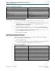
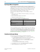
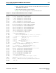
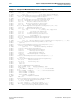
Table Of Contents
- Cyclone V Hard IP for PCI Express User Guide
- Contents
- 1. Datasheet
- 2. Getting Started with the Cyclone V Hard IP for PCI Express
- 3. Getting Started with the Avalon-MM Cyclone Hard IP for PCI Express
- Running Qsys
- Customizing the Cyclone VHard IP for PCI Express IP Core
- Adding the Remaining Components to the Qsys System
- Completing the Connections in Qsys
- Specifying Clocks and Interrupts
- Specifying Exported Interfaces
- Specifying Address Assignments
- Simulating the Example Design
- Simulating the Single DWord Design
- Understanding Channel Placement Guidelines
- Adding Synopsis Design Constraints
- Creating a Quartus II Project
- Compiling the Design
- Programming a Device
- 4. Parameter Settings for the Cyclone V Hard IP for PCI Express
- 5. Parameter Settings for the Avalon-MM Cyclone V Hard IP for PCI Express
- 6. IP Core Architecture
- Key Interfaces
- Protocol Layers
- Multi-Function Support
- PCI Express Avalon-MM Bridge
- Avalon-MM Bridge TLPs
- Avalon-MM-to-PCI Express Write Requests
- Avalon-MM-to-PCI Express Upstream Read Requests
- PCI Express-to-Avalon-MM Read Completions
- PCI Express-to-Avalon-MM Downstream Write Requests
- PCI Express-to-Avalon-MM Downstream Read Requests
- Avalon-MM-to-PCI Express Read Completions
- PCI Express-to-Avalon-MM Address Translation for Endpoints
- Minimizing BAR Sizes and the PCIe Address Space
- Avalon-MM-to-PCI Express Address Translation Algorithm
- Single DWord Completer Endpoint
- 7. IP Core Interfaces
- Cyclone V Hard IP for PCI Express
- Avalon-MM Hard IP for PCI Express
- Physical Layer Interface Signals
- Test Signals
- 8. Register Descriptions
- Configuration Space Register Content
- Altera-Defined Vendor Specific Extended Capability (VSEC)
- PCI Express Avalon-MM Bridge Control Register Access Content
- Avalon-MM to PCI Express Interrupt Registers
- PCI Express Mailbox Registers
- Avalon-MM-to-PCI Express Address Translation Table
- Root Port TLP Data Registers
- Programming Model for Avalon-MM Root Port
- PCI Express to Avalon-MM Interrupt Status and Enable Registers for Root Ports
- PCI Express to Avalon-MM Interrupt Status and Enable Registers for Endpoints
- Avalon-MM Mailbox Registers
- Correspondence between Configuration Space Registers and the PCIe Spec 2.1
- 9. Reset and Clocks
- 10. Transaction Layer Protocol (TLP) Details
- 11. Interrupts
- Interrupts for Endpoints Using the Avalon-ST Application Interface
- Interrupts for Root Ports Using the Avalon-ST Interface to the Application Layer
- Interrupts for Endpoints Using the Avalon-MM Interface to the Application Layer
- Interrupts for End Points Using the Avalon-MM Interface with Multiple MSI/MSI-X Support
- 12. Optional Features
- 13. Flow Control
- 14. Error Handling
- 15. Transceiver PHY IP Reconfiguration
- 16. SDC Timing Constraints
- 17. Testbench and Design Example
- Endpoint Testbench
- Root Port Testbench
- Chaining DMA Design Examples
- Test Driver Module
- Root Port Design Example
- Root Port BFM
- BFM Procedures and Functions
- 18. Debugging
- A. Transaction Layer Packet (TLP) Header Formats
- Additional Information

3–14 Chapter 3: Getting Started with the Avalon-MM Cyclone Hard IP for PCI Express
Simulating the Example Design
Cyclone V Hard IP for PCI Express December 2013 Altera Corporation
User Guide
Example 3–1. Transcript from ModelSim Simulation of Gen1 x4 Endpoint (continued)
# INFO: 37960 ns EP PCI Express Capabilities Register (0002):
# INFO: 37960 ns Capability Version: 2
# I
NFO: 37960 ns Port Type: Native Endpoint
# INFO: 37960 ns EP PCI Express Device Capabilities Register (00008020):
# INFO: 37960 ns Max Payload Supported: 128 Bytes
# I
NFO: 37960 ns Extended Tag: Supported
# INFO: 37960 ns Acceptable L0s Latency: Less Than 64 ns
# INFO: 37960 ns A
cceptable L1 Latency: Less Than 1 us
# INFO: 37960 ns Atte
ntion Button: Not Present
# INFO: 37960 ns Attention Indicator: Not Present
# INFO:
37960 ns Power Indicator: Not Present
# IN
FO: 37960 ns EP PCI Express Link Capabilities Register (01406041):
# I
NFO: 37960 ns Maximum Link Width: x4
# I
NFO: 37960 ns Supported Link Speed: 2.5GT/s
# INFO: 37960 ns L0s Entry: Not Supported
# INFO: 37960 ns L1
Entry: Not Supported
# INFO: 37960 ns L0s Exit
Latency: 2 us to 4 us
# INFO: 37960 ns L1 Exit Latency: Less Than 1 us
# INF
O: 37960 ns Port Number: 01
# INFO: 37960 ns Surprise Dwn Err Report: Not Supported
# INFO: 37960 ns DLL Link Active Report: Not Supported
# INFO
: 37960 ns
# INFO: 37960 ns EP PCI Express Device Capabilities 2 Register (0000001F):
# INFO: 37960 ns Completion Timeout Rnge: ABCD (50us to 64s)
# INFO
: 39512 ns
# INFO: 39512 ns EP PCI Express Device Control Register (0110):
# INFO: 39512 ns Error Reporting Enables: 0
# I
NFO: 39512 ns Relaxed Ordering: Enabled
# INFO: 39512 ns Error Reporting Enables: 0
# INFO: 39512 ns Relaxed Ordering: Enabled
# I
NFO: 39512 ns Max Payload: 128 Bytes
# I
NFO: 39512 ns Extended Tag: Enabled
# INFO
: 39512 ns Max Read Request: 128 Bytes
# INFO
: 39512 ns
# INFO: 39512 ns EP PCI Express Device Status Register (0000):
# INFO: 39512 ns
# IN
FO: 41016 ns EP PCI Express Virtual Channel Capability:
# INFO: 41016 ns Virtual Channel: 1
# INFO: 41016 ns Low Priority VC: 0
# INFO: 41016 ns
# INFO: 46456 ns
# INFO: 46456 ns BAR Address Assignments:
# I
NFO: 46456 ns BAR Size Assigned Address Type
# INFO
: 46456 ns --- ---- ----------------
# INFO: 464
56 ns BAR1:0 4 MBytes 00000001 00000000 Prefetchable
# INFO: 464
56 ns BAR2 32 KBytes 00200000 Non-Prefetchable
# INFO: 46456 ns BAR3 Disabled
# INFO: 46456 ns BAR4 Disabled
# INFO: 46456 ns BAR5 Disabled
# I
NFO: 46456 ns ExpROM Disabled
INFO: 48408 ns
# INFO: 48408 ns Completed configuration of Endpoint BARs.
# INFO: 50008 ns Starting Target Write/Read Test.
# INFO: 50008 ns Target BAR = 0
# INFO: 50008 ns Length = 000512, Start Offset = 000000
# INFO: 54368 ns Target
Write and Read compared okay!
# I
NFO: 54368 ns Starting DMA Read/Write Test.