
User guide
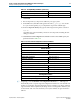
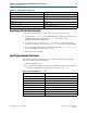


Table Of Contents
- Cyclone V Hard IP for PCI Express User Guide
- Contents
- 1. Datasheet
- 2. Getting Started with the Cyclone V Hard IP for PCI Express
- 3. Getting Started with the Avalon-MM Cyclone Hard IP for PCI Express
- Running Qsys
- Customizing the Cyclone VHard IP for PCI Express IP Core
- Adding the Remaining Components to the Qsys System
- Completing the Connections in Qsys
- Specifying Clocks and Interrupts
- Specifying Exported Interfaces
- Specifying Address Assignments
- Simulating the Example Design
- Simulating the Single DWord Design
- Understanding Channel Placement Guidelines
- Adding Synopsis Design Constraints
- Creating a Quartus II Project
- Compiling the Design
- Programming a Device
- 4. Parameter Settings for the Cyclone V Hard IP for PCI Express
- 5. Parameter Settings for the Avalon-MM Cyclone V Hard IP for PCI Express
- 6. IP Core Architecture
- Key Interfaces
- Protocol Layers
- Multi-Function Support
- PCI Express Avalon-MM Bridge
- Avalon-MM Bridge TLPs
- Avalon-MM-to-PCI Express Write Requests
- Avalon-MM-to-PCI Express Upstream Read Requests
- PCI Express-to-Avalon-MM Read Completions
- PCI Express-to-Avalon-MM Downstream Write Requests
- PCI Express-to-Avalon-MM Downstream Read Requests
- Avalon-MM-to-PCI Express Read Completions
- PCI Express-to-Avalon-MM Address Translation for Endpoints
- Minimizing BAR Sizes and the PCIe Address Space
- Avalon-MM-to-PCI Express Address Translation Algorithm
- Single DWord Completer Endpoint
- 7. IP Core Interfaces
- Cyclone V Hard IP for PCI Express
- Avalon-MM Hard IP for PCI Express
- Physical Layer Interface Signals
- Test Signals
- 8. Register Descriptions
- Configuration Space Register Content
- Altera-Defined Vendor Specific Extended Capability (VSEC)
- PCI Express Avalon-MM Bridge Control Register Access Content
- Avalon-MM to PCI Express Interrupt Registers
- PCI Express Mailbox Registers
- Avalon-MM-to-PCI Express Address Translation Table
- Root Port TLP Data Registers
- Programming Model for Avalon-MM Root Port
- PCI Express to Avalon-MM Interrupt Status and Enable Registers for Root Ports
- PCI Express to Avalon-MM Interrupt Status and Enable Registers for Endpoints
- Avalon-MM Mailbox Registers
- Correspondence between Configuration Space Registers and the PCIe Spec 2.1
- 9. Reset and Clocks
- 10. Transaction Layer Protocol (TLP) Details
- 11. Interrupts
- Interrupts for Endpoints Using the Avalon-ST Application Interface
- Interrupts for Root Ports Using the Avalon-ST Interface to the Application Layer
- Interrupts for Endpoints Using the Avalon-MM Interface to the Application Layer
- Interrupts for End Points Using the Avalon-MM Interface with Multiple MSI/MSI-X Support
- 12. Optional Features
- 13. Flow Control
- 14. Error Handling
- 15. Transceiver PHY IP Reconfiguration
- 16. SDC Timing Constraints
- 17. Testbench and Design Example
- Endpoint Testbench
- Root Port Testbench
- Chaining DMA Design Examples
- Test Driver Module
- Root Port Design Example
- Root Port BFM
- BFM Procedures and Functions
- 18. Debugging
- A. Transaction Layer Packet (TLP) Header Formats
- Additional Information
Chapter 3: Getting Started with the Avalon-MM Cyclone Hard IP for PCI Express 3–7
Adding the Remaining Components to the Qsys System
December 2013 Altera Corporation Cyclone V Hard IP for PCI Express
User Guide
7. Click Finish.
8. The On-chip memory component is added to your Qsys system.
9. On the File menu, click Save and type the file name
ep_g1x4.qsys
. You should
save your work frequently as you complete the steps in this walkthrough.
10. On the Component Library tab, type the following text string in the search box:
recon r
Qsys filters the component library and shows all components matching the text
string you entered.
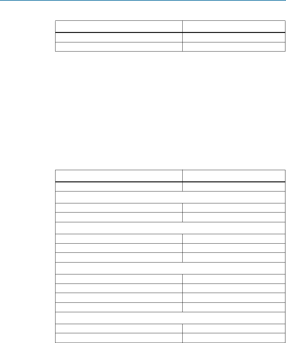
11. Click Transceiver Reconfiguration Controller and then click +Add. Specify the
parameters listed in Table 3–10.
1 Originally, you set the Number of reconfiguration interfaces to
5
. Although you
must initially create a separate logical reconfiguration interface for each channel and
TX PLL in your design, when the Quartus II software compiles your design, it merges
logical channels. After compilation, the design has two reconfiguration interfaces, one
for the TX PLL and one for the channels; however, the number of logical channels is
still five.
Enable In-System Memory Content Editor feature D Turn off this option
Instance ID Not required
Table 3–10. Transceiver Reconfiguration Controller Parameters
Parameter Value
Device family
Interface Bundles
Number of reconfiguration interfaces 5
Optional interface grouping Leave this entry blank
Transceiver Calibration Functions
Enable offset cancellation Leave this option on
Enable PLL calibration Leave this option on
Create optional calibration status ports Leave this option off
Analog Features
Enable Analog controls Turn this option on
Enable EyeQ block Leave this option off
Enable decision feedback equalizer (DFE) block Leave this option off
Enable AEQ block Leave this option off
Reconfiguration Features
Enable channel/PLL reconfiguration Leave this option off
Enable PLL reconfiguration support block Leave this option off
Table 3–9. On-Chip Memory Parameters (Part 2 of 2)
Parameter Value