
User guide

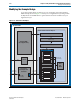
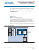
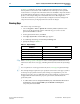
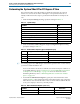
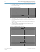
Table Of Contents
- Cyclone V Hard IP for PCI Express User Guide
- Contents
- 1. Datasheet
- 2. Getting Started with the Cyclone V Hard IP for PCI Express
- 3. Getting Started with the Avalon-MM Cyclone Hard IP for PCI Express
- Running Qsys
- Customizing the Cyclone VHard IP for PCI Express IP Core
- Adding the Remaining Components to the Qsys System
- Completing the Connections in Qsys
- Specifying Clocks and Interrupts
- Specifying Exported Interfaces
- Specifying Address Assignments
- Simulating the Example Design
- Simulating the Single DWord Design
- Understanding Channel Placement Guidelines
- Adding Synopsis Design Constraints
- Creating a Quartus II Project
- Compiling the Design
- Programming a Device
- 4. Parameter Settings for the Cyclone V Hard IP for PCI Express
- 5. Parameter Settings for the Avalon-MM Cyclone V Hard IP for PCI Express
- 6. IP Core Architecture
- Key Interfaces
- Protocol Layers
- Multi-Function Support
- PCI Express Avalon-MM Bridge
- Avalon-MM Bridge TLPs
- Avalon-MM-to-PCI Express Write Requests
- Avalon-MM-to-PCI Express Upstream Read Requests
- PCI Express-to-Avalon-MM Read Completions
- PCI Express-to-Avalon-MM Downstream Write Requests
- PCI Express-to-Avalon-MM Downstream Read Requests
- Avalon-MM-to-PCI Express Read Completions
- PCI Express-to-Avalon-MM Address Translation for Endpoints
- Minimizing BAR Sizes and the PCIe Address Space
- Avalon-MM-to-PCI Express Address Translation Algorithm
- Single DWord Completer Endpoint
- 7. IP Core Interfaces
- Cyclone V Hard IP for PCI Express
- Avalon-MM Hard IP for PCI Express
- Physical Layer Interface Signals
- Test Signals
- 8. Register Descriptions
- Configuration Space Register Content
- Altera-Defined Vendor Specific Extended Capability (VSEC)
- PCI Express Avalon-MM Bridge Control Register Access Content
- Avalon-MM to PCI Express Interrupt Registers
- PCI Express Mailbox Registers
- Avalon-MM-to-PCI Express Address Translation Table
- Root Port TLP Data Registers
- Programming Model for Avalon-MM Root Port
- PCI Express to Avalon-MM Interrupt Status and Enable Registers for Root Ports
- PCI Express to Avalon-MM Interrupt Status and Enable Registers for Endpoints
- Avalon-MM Mailbox Registers
- Correspondence between Configuration Space Registers and the PCIe Spec 2.1
- 9. Reset and Clocks
- 10. Transaction Layer Protocol (TLP) Details
- 11. Interrupts
- Interrupts for Endpoints Using the Avalon-ST Application Interface
- Interrupts for Root Ports Using the Avalon-ST Interface to the Application Layer
- Interrupts for Endpoints Using the Avalon-MM Interface to the Application Layer
- Interrupts for End Points Using the Avalon-MM Interface with Multiple MSI/MSI-X Support
- 12. Optional Features
- 13. Flow Control
- 14. Error Handling
- 15. Transceiver PHY IP Reconfiguration
- 16. SDC Timing Constraints
- 17. Testbench and Design Example
- Endpoint Testbench
- Root Port Testbench
- Chaining DMA Design Examples
- Test Driver Module
- Root Port Design Example
- Root Port BFM
- BFM Procedures and Functions
- 18. Debugging
- A. Transaction Layer Packet (TLP) Header Formats
- Additional Information
3–6 Chapter 3: Getting Started with the Avalon-MM Cyclone Hard IP for PCI Express
Adding the Remaining Components to the Qsys System
Cyclone V Hard IP for PCI Express December 2013 Altera Corporation
User Guide
3. In the DMA Controller parameter editor, specify the parameters and conditions
listed in the following table.
4. Click Finish. The DMA Controller module is added to your Qsys system.
5. On the Component Library tab, type the following text string in the search box:
On Chip r
Qsys filters the component library and shows all components matching the text
string you entered.
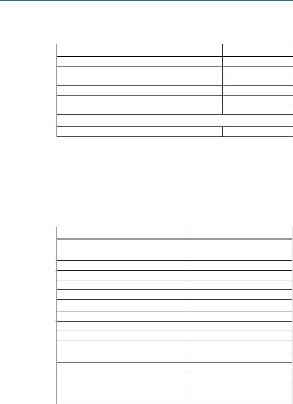
6. Click On-Chip Memory (RAM or ROM) and then click +Add. Specify the
parameters listed in the following table.
Table 3–8. DMA Controller Parameters
Parameter Value
Width of the DMA length register 13
Enable burst transfers Turn on this option
Maximum burst size Select 128
Data transfer FIFO depth Select 32
Construct FIFO from registers Turn off this option
Construct FIFO from embedded memory blocks Turn on this option
Advanced
Allowed Transactions Turn on all options
Table 3–9. On-Chip Memory Parameters (Part 1 of 2)
Parameter Value
Memory Type
Type Select RAM (Writeable)
Dual-port access Turn off this option
Single clock option Not applicable
Read During Write Mode Not applicable
Block type
Auto
Size
Data width 64
Total memory size 4096 Bytes
Minimize memory block usage (may impact f
MAX
) Not applicable
Read latency
Slave s1 latency 1
Slave s2 latency Not applicable
Memory initialization
Initialize memory content Turn on this option
Enable non-default initialization file Turn off this option