
User guide


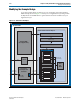

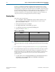
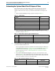

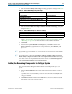
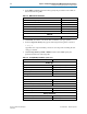
Table Of Contents
- Cyclone V Hard IP for PCI Express User Guide
- Contents
- 1. Datasheet
- 2. Getting Started with the Cyclone V Hard IP for PCI Express
- 3. Getting Started with the Avalon-MM Cyclone Hard IP for PCI Express
- Running Qsys
- Customizing the Cyclone VHard IP for PCI Express IP Core
- Adding the Remaining Components to the Qsys System
- Completing the Connections in Qsys
- Specifying Clocks and Interrupts
- Specifying Exported Interfaces
- Specifying Address Assignments
- Simulating the Example Design
- Simulating the Single DWord Design
- Understanding Channel Placement Guidelines
- Adding Synopsis Design Constraints
- Creating a Quartus II Project
- Compiling the Design
- Programming a Device
- 4. Parameter Settings for the Cyclone V Hard IP for PCI Express
- 5. Parameter Settings for the Avalon-MM Cyclone V Hard IP for PCI Express
- 6. IP Core Architecture
- Key Interfaces
- Protocol Layers
- Multi-Function Support
- PCI Express Avalon-MM Bridge
- Avalon-MM Bridge TLPs
- Avalon-MM-to-PCI Express Write Requests
- Avalon-MM-to-PCI Express Upstream Read Requests
- PCI Express-to-Avalon-MM Read Completions
- PCI Express-to-Avalon-MM Downstream Write Requests
- PCI Express-to-Avalon-MM Downstream Read Requests
- Avalon-MM-to-PCI Express Read Completions
- PCI Express-to-Avalon-MM Address Translation for Endpoints
- Minimizing BAR Sizes and the PCIe Address Space
- Avalon-MM-to-PCI Express Address Translation Algorithm
- Single DWord Completer Endpoint
- 7. IP Core Interfaces
- Cyclone V Hard IP for PCI Express
- Avalon-MM Hard IP for PCI Express
- Physical Layer Interface Signals
- Test Signals
- 8. Register Descriptions
- Configuration Space Register Content
- Altera-Defined Vendor Specific Extended Capability (VSEC)
- PCI Express Avalon-MM Bridge Control Register Access Content
- Avalon-MM to PCI Express Interrupt Registers
- PCI Express Mailbox Registers
- Avalon-MM-to-PCI Express Address Translation Table
- Root Port TLP Data Registers
- Programming Model for Avalon-MM Root Port
- PCI Express to Avalon-MM Interrupt Status and Enable Registers for Root Ports
- PCI Express to Avalon-MM Interrupt Status and Enable Registers for Endpoints
- Avalon-MM Mailbox Registers
- Correspondence between Configuration Space Registers and the PCIe Spec 2.1
- 9. Reset and Clocks
- 10. Transaction Layer Protocol (TLP) Details
- 11. Interrupts
- Interrupts for Endpoints Using the Avalon-ST Application Interface
- Interrupts for Root Ports Using the Avalon-ST Interface to the Application Layer
- Interrupts for Endpoints Using the Avalon-MM Interface to the Application Layer
- Interrupts for End Points Using the Avalon-MM Interface with Multiple MSI/MSI-X Support
- 12. Optional Features
- 13. Flow Control
- 14. Error Handling
- 15. Transceiver PHY IP Reconfiguration
- 16. SDC Timing Constraints
- 17. Testbench and Design Example
- Endpoint Testbench
- Root Port Testbench
- Chaining DMA Design Examples
- Test Driver Module
- Root Port Design Example
- Root Port BFM
- BFM Procedures and Functions
- 18. Debugging
- A. Transaction Layer Packet (TLP) Header Formats
- Additional Information
Chapter 3: Getting Started with the Avalon-MM Cyclone Hard IP for PCI Express 3–3
Customizing the Cyclone VHard IP for PCI Express IP Core
December 2013 Altera Corporation Cyclone V Hard IP for PCI Express
User Guide
Customizing the Cyclone VHard IP for PCI Express IP Core
The parameter editor uses bold headings to divide the parameters into separate
sections. You can use the scroll bar on the right to view parameters that are not
initially visible. Follow these steps to parameterize the Hard IP for PCI Express IP
core:
1. Under the System Settings heading, specify the settings in Table 3–2.
2. Under the PCI Base Address Registers (Type 0 Configuration Space) heading,
specify the settings in Table 3–3.
1 For existing Qsys Avalon-MM designs created in the Quartus II 12.0 or earlier release,
you must re-enable the BARs in 12.1.
For more information about the use of BARs to translate PCI Express addresses to
Avalon-MM addresses, refer to “PCI Express-to-Avalon-MM Address Translation
for Endpoints for 32-Bit Bridge” on page 7–20. For more information about
minimizing BAR sizes, refer to “Minimizing BAR Sizes and the PCIe Address
Space” on page 7–21.
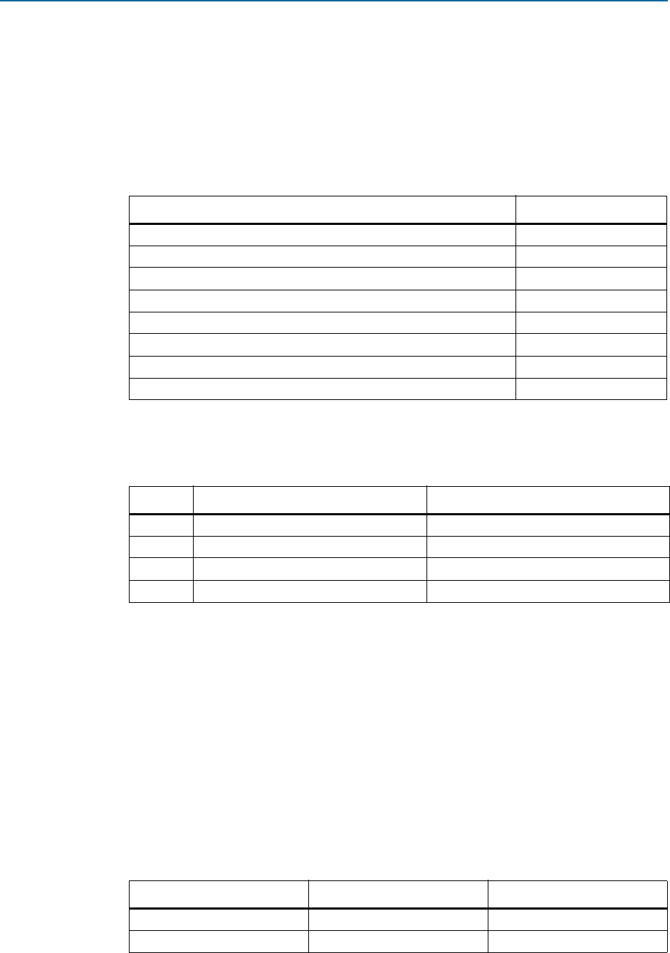
3. For the Device Identification Registers, specify the values listed in the center
column of Table 3–4. The right-hand column of this table lists the value assigned to
Altera devices. You must use the Altera values to run the Altera testbench. Be sure
to use your company’s values for your final product.
Table 3–2. System Settings
Parameter Value
Number of lanes ×4
Lane rate Gen1 (2.5 Gbps)
Port type Native endpoint
RX buffer credit allocation – performance for received requests Low
Reference clock frequency 100 MHz
Use 62.5 MHz application clock Off
Enable configuration via the PCIe link Off
ATX PLL Off
Table 3–3. PCI Base Address Registers (Type 0 Configuration Space)
BAR BAR Type BAR Size
0 64-bit Prefetchable Memory 0
1 Not used 0
2 32 bit Non-Prefetchable 0
3–5 Not used 0
Table 3–4. Device Identification Registers (Part 1 of 2)
Parameter
Value
Altera Value
Vendor ID
0x00000000
0x00001172
Device ID
0x00000001
0x0000E001