
User guide


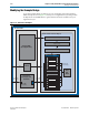

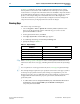
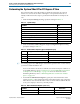
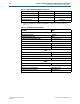
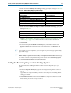
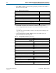
Table Of Contents
- Cyclone V Hard IP for PCI Express User Guide
- Contents
- 1. Datasheet
- 2. Getting Started with the Cyclone V Hard IP for PCI Express
- 3. Getting Started with the Avalon-MM Cyclone Hard IP for PCI Express
- Running Qsys
- Customizing the Cyclone VHard IP for PCI Express IP Core
- Adding the Remaining Components to the Qsys System
- Completing the Connections in Qsys
- Specifying Clocks and Interrupts
- Specifying Exported Interfaces
- Specifying Address Assignments
- Simulating the Example Design
- Simulating the Single DWord Design
- Understanding Channel Placement Guidelines
- Adding Synopsis Design Constraints
- Creating a Quartus II Project
- Compiling the Design
- Programming a Device
- 4. Parameter Settings for the Cyclone V Hard IP for PCI Express
- 5. Parameter Settings for the Avalon-MM Cyclone V Hard IP for PCI Express
- 6. IP Core Architecture
- Key Interfaces
- Protocol Layers
- Multi-Function Support
- PCI Express Avalon-MM Bridge
- Avalon-MM Bridge TLPs
- Avalon-MM-to-PCI Express Write Requests
- Avalon-MM-to-PCI Express Upstream Read Requests
- PCI Express-to-Avalon-MM Read Completions
- PCI Express-to-Avalon-MM Downstream Write Requests
- PCI Express-to-Avalon-MM Downstream Read Requests
- Avalon-MM-to-PCI Express Read Completions
- PCI Express-to-Avalon-MM Address Translation for Endpoints
- Minimizing BAR Sizes and the PCIe Address Space
- Avalon-MM-to-PCI Express Address Translation Algorithm
- Single DWord Completer Endpoint
- 7. IP Core Interfaces
- Cyclone V Hard IP for PCI Express
- Avalon-MM Hard IP for PCI Express
- Physical Layer Interface Signals
- Test Signals
- 8. Register Descriptions
- Configuration Space Register Content
- Altera-Defined Vendor Specific Extended Capability (VSEC)
- PCI Express Avalon-MM Bridge Control Register Access Content
- Avalon-MM to PCI Express Interrupt Registers
- PCI Express Mailbox Registers
- Avalon-MM-to-PCI Express Address Translation Table
- Root Port TLP Data Registers
- Programming Model for Avalon-MM Root Port
- PCI Express to Avalon-MM Interrupt Status and Enable Registers for Root Ports
- PCI Express to Avalon-MM Interrupt Status and Enable Registers for Endpoints
- Avalon-MM Mailbox Registers
- Correspondence between Configuration Space Registers and the PCIe Spec 2.1
- 9. Reset and Clocks
- 10. Transaction Layer Protocol (TLP) Details
- 11. Interrupts
- Interrupts for Endpoints Using the Avalon-ST Application Interface
- Interrupts for Root Ports Using the Avalon-ST Interface to the Application Layer
- Interrupts for Endpoints Using the Avalon-MM Interface to the Application Layer
- Interrupts for End Points Using the Avalon-MM Interface with Multiple MSI/MSI-X Support
- 12. Optional Features
- 13. Flow Control
- 14. Error Handling
- 15. Transceiver PHY IP Reconfiguration
- 16. SDC Timing Constraints
- 17. Testbench and Design Example
- Endpoint Testbench
- Root Port Testbench
- Chaining DMA Design Examples
- Test Driver Module
- Root Port Design Example
- Root Port BFM
- BFM Procedures and Functions
- 18. Debugging
- A. Transaction Layer Packet (TLP) Header Formats
- Additional Information

Chapter 2: Getting Started with the Cyclone V Hard IP for PCI Express 2–15
Compiling the Design in the Qsys Design Flow
December 2013 Altera Corporation Cyclone V Hard IP for PCI Express
User Guide
Compiling the Design in the MegaWizard Plug-In Manager Design Flow
Before compiling the complete example design in the Quartus II software, you must
add the example design files that you generated in Qsys to your Quartus II project.
The Quartus II IP File (.qip) lists all files necessary to compile the project.
Follow these steps to add the Quartus II IP File (.qip) to the project:
1. On the Project menu, select Add/Remove Files in Project.
2. Click the browse button next the File name box and browse to the
gen1_x4_example_design/altera_pcie_sv_hip_ast/pcie_de_gen1_x4_ast64/
synthesis/ directory.
3. In the Files of type list, Click pcie_de_ge1_x4_ast64.qip and then click Open.
4. On the Add Files page, click Add, then click OK.
5. Add the Synopsys Design Constraints (SDC) shown in Example 2–2, to the
top-level design file for your Quartus II project.
6. On the Processing menu, select Start Compilation.
Compiling the Design in the Qsys Design Flow
To compile the Qsys design example in the Quartus II software, you must create a
Quartus II project and add your Qsys files to that project.
Complete the following steps to create your Quartus II project:
1. From the Windows Start Menu, choose Programs > Altera > Quartus II 13.1 to run
the Quartus II software.
Example 2–2. Synopsys Design Constraint
create_clock -period “100 MHz” -name {refclk_pci_express} {*refclk_*}
derive_pll_clocks
derive_clock_uncertainty
######################################################################
# PHY IP reconfig controller constraints
# Set reconfig_xcvr clock
# Modify to match the actual clock pin name
# used for this clock, and also changed to have the correct period set
create_clock -period "125 MHz" -name {reconfig_xcvr_clk}
{*reconfig_xcvr_clk*}
######################################################################
# HIP Soft reset controller SDC constraints
set_false_path -to [get_registers
*altpcie_rs_serdes|fifo_err_sync_r[0]]
set_false_path -from [get_registers *sv_xcvr_pipe_native*] -to
[get_registers *altpcie_rs_serdes|*]
# Hard IP testin pins SDC constraints
set_false_path -from [get_pins -compatibilitly_mode *hip_ctrl*]