
User guide
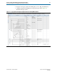
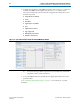
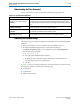
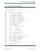
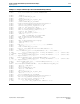
Table Of Contents
- Cyclone V Hard IP for PCI Express User Guide
- Contents
- 1. Datasheet
- 2. Getting Started with the Cyclone V Hard IP for PCI Express
- 3. Getting Started with the Avalon-MM Cyclone Hard IP for PCI Express
- Running Qsys
- Customizing the Cyclone VHard IP for PCI Express IP Core
- Adding the Remaining Components to the Qsys System
- Completing the Connections in Qsys
- Specifying Clocks and Interrupts
- Specifying Exported Interfaces
- Specifying Address Assignments
- Simulating the Example Design
- Simulating the Single DWord Design
- Understanding Channel Placement Guidelines
- Adding Synopsis Design Constraints
- Creating a Quartus II Project
- Compiling the Design
- Programming a Device
- 4. Parameter Settings for the Cyclone V Hard IP for PCI Express
- 5. Parameter Settings for the Avalon-MM Cyclone V Hard IP for PCI Express
- 6. IP Core Architecture
- Key Interfaces
- Protocol Layers
- Multi-Function Support
- PCI Express Avalon-MM Bridge
- Avalon-MM Bridge TLPs
- Avalon-MM-to-PCI Express Write Requests
- Avalon-MM-to-PCI Express Upstream Read Requests
- PCI Express-to-Avalon-MM Read Completions
- PCI Express-to-Avalon-MM Downstream Write Requests
- PCI Express-to-Avalon-MM Downstream Read Requests
- Avalon-MM-to-PCI Express Read Completions
- PCI Express-to-Avalon-MM Address Translation for Endpoints
- Minimizing BAR Sizes and the PCIe Address Space
- Avalon-MM-to-PCI Express Address Translation Algorithm
- Single DWord Completer Endpoint
- 7. IP Core Interfaces
- Cyclone V Hard IP for PCI Express
- Avalon-MM Hard IP for PCI Express
- Physical Layer Interface Signals
- Test Signals
- 8. Register Descriptions
- Configuration Space Register Content
- Altera-Defined Vendor Specific Extended Capability (VSEC)
- PCI Express Avalon-MM Bridge Control Register Access Content
- Avalon-MM to PCI Express Interrupt Registers
- PCI Express Mailbox Registers
- Avalon-MM-to-PCI Express Address Translation Table
- Root Port TLP Data Registers
- Programming Model for Avalon-MM Root Port
- PCI Express to Avalon-MM Interrupt Status and Enable Registers for Root Ports
- PCI Express to Avalon-MM Interrupt Status and Enable Registers for Endpoints
- Avalon-MM Mailbox Registers
- Correspondence between Configuration Space Registers and the PCIe Spec 2.1
- 9. Reset and Clocks
- 10. Transaction Layer Protocol (TLP) Details
- 11. Interrupts
- Interrupts for Endpoints Using the Avalon-ST Application Interface
- Interrupts for Root Ports Using the Avalon-ST Interface to the Application Layer
- Interrupts for Endpoints Using the Avalon-MM Interface to the Application Layer
- Interrupts for End Points Using the Avalon-MM Interface with Multiple MSI/MSI-X Support
- 12. Optional Features
- 13. Flow Control
- 14. Error Handling
- 15. Transceiver PHY IP Reconfiguration
- 16. SDC Timing Constraints
- 17. Testbench and Design Example
- Endpoint Testbench
- Root Port Testbench
- Chaining DMA Design Examples
- Test Driver Module
- Root Port Design Example
- Root Port BFM
- BFM Procedures and Functions
- 18. Debugging
- A. Transaction Layer Packet (TLP) Header Formats
- Additional Information

2–14 Chapter 2: Getting Started with the Cyclone V Hard IP for PCI Express
Qsys Design Flow
Cyclone V Hard IP for PCI Express December 2013 Altera Corporation
User Guide
Understanding Channel Placement Guidelines
f Refer to “Channel Placement for ×1 Variants” on page 7–47 for more information
about channel placement for ×1 and ×4 variants.For more information about
Cyclone V transceivers refer to the “PCIe Supported Configurations and Placement
Guides” section in the Transceiver Protocol Configurations in Cyclone V Devices.
Example 2-1Excerpts from Transcript of Successful Simulation Run (continued)
# INFO: 96005 ns multi_message_enable = 0x0002
# INFO: 96005 ns msi_number = 0001
# INFO: 96005 ns msi_tr
affic_class = 0000
# INFO: 96005 ns ---------
# INFO: 96005 ns TASK:dma_set_header WRITE
# INFO
: 96005 ns Writing Descriptor header
# INFO: 960
45 ns data content of the DT header
# INFO
: 96045 ns
# INFO: 96045 ns Shared Memory Data Display:
# INFO: 96045 ns Address Data
# INFO: 96045 ns ------- ----
# INFO: 96045 ns 00000800 10100003 00000000 00000800 CAFEFADE
#
INFO: 96045 ns ---------
# INFO: 96045 ns TASK:dma_set_rclast
# INFO: 96045 ns Start WRITE DMA : RC issues MWr (RCLast=0002)
# INFO: 96061 ns ---------
# INFO: 96073 ns TASK:msi_poll Po
lling MSI Address:07F0---> Data:FADE......
# INFO: 96257 ns TASK:rcmem_poll Polling RC Address0000080C current data
(0000FADE) expected data (00000002)
# INFO: 101457 ns TASK:rcmem_poll Polling RC Address0000080C current data
(00000000) expected data (00000002)
# INFO: 105177 ns TASK:msi_poll Received DMA Write MSI(0000) : B0FD
# I
NFO: 105257 ns TASK:rcmem_poll Polling RC Address0000080C current data
(00000002) expected data (00000002)
# INFO: 105257 ns TASK:rcmem_poll ---> Received Expected Data (00000002)
# INFO: 105265 ns ---------
# INFO: 105265 ns Completed DMA Write
# INFO
: 105265 ns ---------
# INFO: 105265 ns TASK:check_dma_data
# INFO: 105265 ns Passed : 0644 identical dwords.
# INFO
: 105265 ns ---------
# INFO: 105265 ns TASK:downstream_loop
# INFO: 107897 ns Passed: 0004 same bytes in BFM mem addr 0x00000040 and 0x00000840
# INFO: 110409 ns Passed: 0008 same bytes in BFM mem addr 0x00000040 and 0x00000840
# INFO: 113
033 ns Passed: 0012 same bytes in BFM mem addr 0x00000040 and 0x00000840
# INFO: 115665 ns Passed: 0016 same bytes in BFM mem addr 0x00000040 and 0x00000840
# INFO: 118305 ns Passed: 0020 same bytes in BFM mem addr 0x00000040 and 0x00000840
# INFO: 120
937 ns Passed: 0024 same bytes in BFM mem addr 0x00000040 and 0x00000840
# INFO: 123577 ns Passed: 0028 same bytes in BFM mem addr 0x00000040 and 0x00000840
# INFO: 126
241 ns Passed: 0032 same bytes in BFM mem addr 0x00000040 and 0x00000840
# INFO: 128897 ns Passed: 0036 same bytes in BFM mem addr 0x00000040 and 0x00000840
# INFO: 131545 ns Passed: 0040 same bytes in BFM mem addr 0x00000040 and 0x00000840
# SUCCESS: Simulation stopped due to successful completion!