
User guide

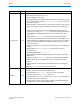
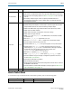
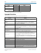


Table Of Contents
- Cyclone V Hard IP for PCI Express User Guide
- Contents
- 1. Datasheet
- 2. Getting Started with the Cyclone V Hard IP for PCI Express
- 3. Getting Started with the Avalon-MM Cyclone Hard IP for PCI Express
- Running Qsys
- Customizing the Cyclone VHard IP for PCI Express IP Core
- Adding the Remaining Components to the Qsys System
- Completing the Connections in Qsys
- Specifying Clocks and Interrupts
- Specifying Exported Interfaces
- Specifying Address Assignments
- Simulating the Example Design
- Simulating the Single DWord Design
- Understanding Channel Placement Guidelines
- Adding Synopsis Design Constraints
- Creating a Quartus II Project
- Compiling the Design
- Programming a Device
- 4. Parameter Settings for the Cyclone V Hard IP for PCI Express
- 5. Parameter Settings for the Avalon-MM Cyclone V Hard IP for PCI Express
- 6. IP Core Architecture
- Key Interfaces
- Protocol Layers
- Multi-Function Support
- PCI Express Avalon-MM Bridge
- Avalon-MM Bridge TLPs
- Avalon-MM-to-PCI Express Write Requests
- Avalon-MM-to-PCI Express Upstream Read Requests
- PCI Express-to-Avalon-MM Read Completions
- PCI Express-to-Avalon-MM Downstream Write Requests
- PCI Express-to-Avalon-MM Downstream Read Requests
- Avalon-MM-to-PCI Express Read Completions
- PCI Express-to-Avalon-MM Address Translation for Endpoints
- Minimizing BAR Sizes and the PCIe Address Space
- Avalon-MM-to-PCI Express Address Translation Algorithm
- Single DWord Completer Endpoint
- 7. IP Core Interfaces
- Cyclone V Hard IP for PCI Express
- Avalon-MM Hard IP for PCI Express
- Physical Layer Interface Signals
- Test Signals
- 8. Register Descriptions
- Configuration Space Register Content
- Altera-Defined Vendor Specific Extended Capability (VSEC)
- PCI Express Avalon-MM Bridge Control Register Access Content
- Avalon-MM to PCI Express Interrupt Registers
- PCI Express Mailbox Registers
- Avalon-MM-to-PCI Express Address Translation Table
- Root Port TLP Data Registers
- Programming Model for Avalon-MM Root Port
- PCI Express to Avalon-MM Interrupt Status and Enable Registers for Root Ports
- PCI Express to Avalon-MM Interrupt Status and Enable Registers for Endpoints
- Avalon-MM Mailbox Registers
- Correspondence between Configuration Space Registers and the PCIe Spec 2.1
- 9. Reset and Clocks
- 10. Transaction Layer Protocol (TLP) Details
- 11. Interrupts
- Interrupts for Endpoints Using the Avalon-ST Application Interface
- Interrupts for Root Ports Using the Avalon-ST Interface to the Application Layer
- Interrupts for Endpoints Using the Avalon-MM Interface to the Application Layer
- Interrupts for End Points Using the Avalon-MM Interface with Multiple MSI/MSI-X Support
- 12. Optional Features
- 13. Flow Control
- 14. Error Handling
- 15. Transceiver PHY IP Reconfiguration
- 16. SDC Timing Constraints
- 17. Testbench and Design Example
- Endpoint Testbench
- Root Port Testbench
- Chaining DMA Design Examples
- Test Driver Module
- Root Port Design Example
- Root Port BFM
- BFM Procedures and Functions
- 18. Debugging
- A. Transaction Layer Packet (TLP) Header Formats
- Additional Information
Chapter : A–3
TLP Packet Format with Data Payload
December 2013 Altera Corporation Cyclone V Hard IP for PCI Express
User Guide
TLP Packet Format with Data Payload
Table A–10 through Table A–16 show the content for TLPs with a data payload.
Table A–10. Memory Write Request, 32-Bit Addressing
+0 +1 +2 +3
76543210765432107 6 54321076543210
Byte 0 010000000
TC
0000
TD EP
Attr
AT Length
Byte 4
Requester ID Tag Last BE First BE
Byte 8
Address[31:2]
00
Byte 12 Reserved
Table A–11. Memory Write Request, 64-Bit Addressing
+0 +1 +2 +3
76543210765432107 6 5 4 321076543210
Byte 0 011000000
TC
0000
TD EP
Attr
AT Length
Byte 4
Requester ID Tag Last BE First BE
Byte 8
Address[63:32]
Byte 12
Address[31:2]
00
Table A–12. Configuration Write Request Root Port (Type 1)
+0 +1 +2 +3
76543210765432107 6 5 4321076543210
Byte 0 R100010100000000
TD EP
00
AT
0000000001
Byte 4
Requester ID Tag
0000
First BE
Byte 8
Bus Number Device No
0000
Ext Reg Register No
00
Byte 12 Reserved
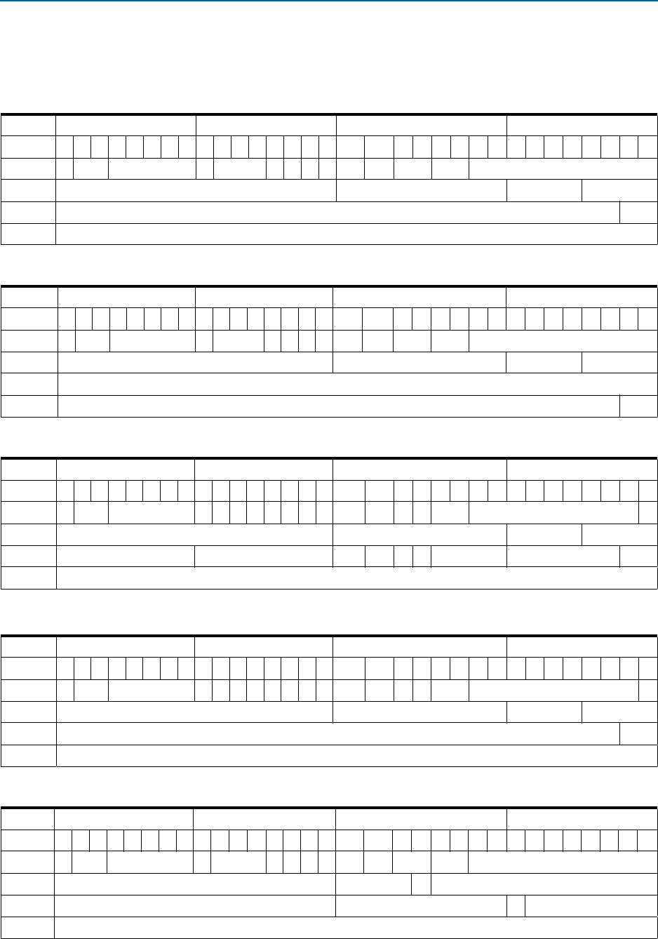
Table A–13. I/O Write Request
+0 +1 +2 +3
76543210765432107 6 5 4321076543210
Byte 0 0100001000000000
TD EP
00
AT
0000000001
Byte 4
Requester ID Tag
0000
First BE
Byte 8
Address[31:2]
00
Byte 12 Reserved
Table A–14. Completion with Data
+0 +1 +2 +3
76543210765432107 6 54321076543210
Byte 0 010010100
TC
0000
TD EP
Attr
AT Length
Byte 4
Completer ID Status B Byte Count
Byte 8
Requester ID Tag
0
Lower Address
Byte 12 Reserved