
User guide

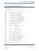
Table Of Contents
- Cyclone V Hard IP for PCI Express User Guide
- Contents
- 1. Datasheet
- 2. Getting Started with the Cyclone V Hard IP for PCI Express
- 3. Getting Started with the Avalon-MM Cyclone Hard IP for PCI Express
- Running Qsys
- Customizing the Cyclone VHard IP for PCI Express IP Core
- Adding the Remaining Components to the Qsys System
- Completing the Connections in Qsys
- Specifying Clocks and Interrupts
- Specifying Exported Interfaces
- Specifying Address Assignments
- Simulating the Example Design
- Simulating the Single DWord Design
- Understanding Channel Placement Guidelines
- Adding Synopsis Design Constraints
- Creating a Quartus II Project
- Compiling the Design
- Programming a Device
- 4. Parameter Settings for the Cyclone V Hard IP for PCI Express
- 5. Parameter Settings for the Avalon-MM Cyclone V Hard IP for PCI Express
- 6. IP Core Architecture
- Key Interfaces
- Protocol Layers
- Multi-Function Support
- PCI Express Avalon-MM Bridge
- Avalon-MM Bridge TLPs
- Avalon-MM-to-PCI Express Write Requests
- Avalon-MM-to-PCI Express Upstream Read Requests
- PCI Express-to-Avalon-MM Read Completions
- PCI Express-to-Avalon-MM Downstream Write Requests
- PCI Express-to-Avalon-MM Downstream Read Requests
- Avalon-MM-to-PCI Express Read Completions
- PCI Express-to-Avalon-MM Address Translation for Endpoints
- Minimizing BAR Sizes and the PCIe Address Space
- Avalon-MM-to-PCI Express Address Translation Algorithm
- Single DWord Completer Endpoint
- 7. IP Core Interfaces
- Cyclone V Hard IP for PCI Express
- Avalon-MM Hard IP for PCI Express
- Physical Layer Interface Signals
- Test Signals
- 8. Register Descriptions
- Configuration Space Register Content
- Altera-Defined Vendor Specific Extended Capability (VSEC)
- PCI Express Avalon-MM Bridge Control Register Access Content
- Avalon-MM to PCI Express Interrupt Registers
- PCI Express Mailbox Registers
- Avalon-MM-to-PCI Express Address Translation Table
- Root Port TLP Data Registers
- Programming Model for Avalon-MM Root Port
- PCI Express to Avalon-MM Interrupt Status and Enable Registers for Root Ports
- PCI Express to Avalon-MM Interrupt Status and Enable Registers for Endpoints
- Avalon-MM Mailbox Registers
- Correspondence between Configuration Space Registers and the PCIe Spec 2.1
- 9. Reset and Clocks
- 10. Transaction Layer Protocol (TLP) Details
- 11. Interrupts
- Interrupts for Endpoints Using the Avalon-ST Application Interface
- Interrupts for Root Ports Using the Avalon-ST Interface to the Application Layer
- Interrupts for Endpoints Using the Avalon-MM Interface to the Application Layer
- Interrupts for End Points Using the Avalon-MM Interface with Multiple MSI/MSI-X Support
- 12. Optional Features
- 13. Flow Control
- 14. Error Handling
- 15. Transceiver PHY IP Reconfiguration
- 16. SDC Timing Constraints
- 17. Testbench and Design Example
- Endpoint Testbench
- Root Port Testbench
- Chaining DMA Design Examples
- Test Driver Module
- Root Port Design Example
- Root Port BFM
- BFM Procedures and Functions
- 18. Debugging
- A. Transaction Layer Packet (TLP) Header Formats
- Additional Information

2–12 Chapter 2: Getting Started with the Cyclone V Hard IP for PCI Express
Qsys Design Flow
Cyclone V Hard IP for PCI Express December 2013 Altera Corporation
User Guide
■ Root Port to Endpoint memory reads and writes
Example 2–1. Excerpts from Transcript of Successful Simulation Run
Time: 56000 Instance: top_chaining_testbench.ep.epmap.pll_250mhz_to_500mhz.
# Time: 0 Instance:
pcie_de_gen1_x8_ast128_tb.dut_pcie_tb.genblk1.genblk1.altpcietb_bfm_top_rp.rp.rp.nl00O
0i.Cycloneii_pll.pll1
# Note : Cyclone II PLL locked to incoming clock
# Time: 25000000 Instance:
pcie_de_gen1_x8_ast128_tb.dut_pcie_tb.genblk1.genblk1.altpcietb_bfm_top_rp.rp.rp.nl00O
0i.Cycloneii_pll.pll1
# INFO: 464 ns Completed initial configuration of Root Port.
# INFO: 3661 ns RP LTSSM State: DETECT.ACTIVE
# I
NFO: 3693 ns RP LTSSM State: POLLING.ACTIVE
# INFO:
3905 ns EP LTSSM State: DETECT.ACTIVE
# I
NFO: 4065 ns EP LTSSM State: POLLING.ACTIVE
# I
NFO: 6369 ns EP LTSSM State: POLLING.CONFIG
# I
NFO: 6461 ns RP LTSSM State: POLLING.CONFIG
# INFO: 7
741 ns RP LTSSM State: CONFIG.LINKWIDTH.START
# INFO: 7969 ns EP LTS
SM State: CONFIG.LINKWIDTH.START
# INFO: 8353 ns EP LTSSM State: CONFIG.LINKWIDTH.ACCEPT
# I
NFO: 8781 ns RP LTSSM State: CONFIG.LINKWIDTH.ACCEPT
# INFO: 9537 ns EP LTSSM State: CONFIG.LANENUM.WAIT
# INFO:
9857 ns EP LTSSM State: CONFIG.LANENUM.ACCEPT
# INFO:
9933 ns RP LTSSM State: CONFIG.LANENUM.ACCEPT
# INFO: 10189 ns RP LTSSM State: CO
NFIG.COMPLETE
# INFO: 10689 ns EP LTSSM State: CONFIG.COMPLETE
# INFO: 121
09 ns RP LTSSM State: CONFIG.IDLE
# INFO: 136
97 ns EP LTSSM State: CONFIG.IDLE
# INFO:
13889 ns EP LTSSM State: L0
# INFO: 13981 ns RP LTSSM State: L0
# INFO: 17800 ns Configuring Bus 001, Device 001, Function 00
# INFO:
17800 ns EP Read Only Configuration Registers:
# INFO: 17800 ns Vendor ID: 1172
# INFO: 17800 ns Device ID: E001
# INFO: 17800 ns Revision ID: 01
# INFO: 17800 ns Class Code: FF0000
# INFO: 17800 ns Subs
ystem Vendor ID: 1172
# INFO: 17800 ns Subsystem ID: E001
# INFO: 17800 ns Interrupt Pin: INTA# used
# INFO: 17800 ns
# INFO: 20040 ns PCI MSI Capability Register:
# IN
FO: 20040 ns 64-Bit Address Capable: Supported
# I
NFO: 20040 ns Messages Requested: 4
# INFO
: 20040 ns
#INFO: 31208 ns EP PCI Express Link Status Register (1081):
# INFO: 31208 ns Negotiated Link Width: x8
# INF
O: 31208 ns Slot Clock Config: System Reference Clock Used
# INFO: 33481 ns RP LTSSM State: RECOVERY.RCVRLOCK
# IN
FO: 34321 ns EP LTSSM State: RECOVERY.RCVRLOCK
# INFO: 3
4961 ns EP LTSSM State: RECOVERY.RCVRCFG
# INFO: 3
5161 ns RP LTSSM State: RECOVERY.RCVRCFG
# I
NFO: 36377 ns RP LTSSM State: RECOVERY.IDLE
# I
NFO: 37457 ns EP LTSSM State: RECOVERY.IDLE
# INFO: 37649 ns EP LTSSM State: L0
# INFO: 37737 ns RP LTSSM State: L0
# INFO: 399
44 ns Current Link Speed: 2.5GT/s
# INFO: 58904 ns Completed configuration of Endpoint BARs.
#
INFO: 61288 ns ---------
# INFO: 61288 ns TASK:chained_dma_test
# I
NFO: 61288 ns DMA: Read