
User guide
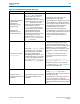
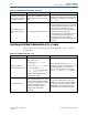
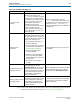
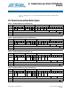
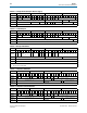
Table Of Contents
- Cyclone V Hard IP for PCI Express User Guide
- Contents
- 1. Datasheet
- 2. Getting Started with the Cyclone V Hard IP for PCI Express
- 3. Getting Started with the Avalon-MM Cyclone Hard IP for PCI Express
- Running Qsys
- Customizing the Cyclone VHard IP for PCI Express IP Core
- Adding the Remaining Components to the Qsys System
- Completing the Connections in Qsys
- Specifying Clocks and Interrupts
- Specifying Exported Interfaces
- Specifying Address Assignments
- Simulating the Example Design
- Simulating the Single DWord Design
- Understanding Channel Placement Guidelines
- Adding Synopsis Design Constraints
- Creating a Quartus II Project
- Compiling the Design
- Programming a Device
- 4. Parameter Settings for the Cyclone V Hard IP for PCI Express
- 5. Parameter Settings for the Avalon-MM Cyclone V Hard IP for PCI Express
- 6. IP Core Architecture
- Key Interfaces
- Protocol Layers
- Multi-Function Support
- PCI Express Avalon-MM Bridge
- Avalon-MM Bridge TLPs
- Avalon-MM-to-PCI Express Write Requests
- Avalon-MM-to-PCI Express Upstream Read Requests
- PCI Express-to-Avalon-MM Read Completions
- PCI Express-to-Avalon-MM Downstream Write Requests
- PCI Express-to-Avalon-MM Downstream Read Requests
- Avalon-MM-to-PCI Express Read Completions
- PCI Express-to-Avalon-MM Address Translation for Endpoints
- Minimizing BAR Sizes and the PCIe Address Space
- Avalon-MM-to-PCI Express Address Translation Algorithm
- Single DWord Completer Endpoint
- 7. IP Core Interfaces
- Cyclone V Hard IP for PCI Express
- Avalon-MM Hard IP for PCI Express
- Physical Layer Interface Signals
- Test Signals
- 8. Register Descriptions
- Configuration Space Register Content
- Altera-Defined Vendor Specific Extended Capability (VSEC)
- PCI Express Avalon-MM Bridge Control Register Access Content
- Avalon-MM to PCI Express Interrupt Registers
- PCI Express Mailbox Registers
- Avalon-MM-to-PCI Express Address Translation Table
- Root Port TLP Data Registers
- Programming Model for Avalon-MM Root Port
- PCI Express to Avalon-MM Interrupt Status and Enable Registers for Root Ports
- PCI Express to Avalon-MM Interrupt Status and Enable Registers for Endpoints
- Avalon-MM Mailbox Registers
- Correspondence between Configuration Space Registers and the PCIe Spec 2.1
- 9. Reset and Clocks
- 10. Transaction Layer Protocol (TLP) Details
- 11. Interrupts
- Interrupts for Endpoints Using the Avalon-ST Application Interface
- Interrupts for Root Ports Using the Avalon-ST Interface to the Application Layer
- Interrupts for Endpoints Using the Avalon-MM Interface to the Application Layer
- Interrupts for End Points Using the Avalon-MM Interface with Multiple MSI/MSI-X Support
- 12. Optional Features
- 13. Flow Control
- 14. Error Handling
- 15. Transceiver PHY IP Reconfiguration
- 16. SDC Timing Constraints
- 17. Testbench and Design Example
- Endpoint Testbench
- Root Port Testbench
- Chaining DMA Design Examples
- Test Driver Module
- Root Port Design Example
- Root Port BFM
- BFM Procedures and Functions
- 18. Debugging
- A. Transaction Layer Packet (TLP) Header Formats
- Additional Information

18–2 Chapter 18: Debugging
Link Training
Cyclone V Hard IP for PCI Express December 2013 Altera Corporation
User Guide
You can use SignalTap II Embedded Logic Analyzer to diagnose the LTSSM state
transitions that are occurring and the PIPE interface. The
ltssmstate[4:0]
bus
encodes the status of LTSSM. The LTSSM state machine reflects the Physical Layer’s
progress through the link training process. For a complete description of the states
these signals encode, refer to “Reset Signals” on page 8–29. When link training
completes successfully and the link is up, the LTSSM should remain stable in the L0
state.
When link issues occur, you can monitor
ltssmstate[4:0]
to determine one of two
cases:
■ The link training fails before reaching the L0 state. Refer to Table 18–1 for possible
causes of the failure to reach L0.
■ The link is initially established (L0), but then stalls with
tx_st_ready
deasserted
for more than 100 cycles. Refer to Table 18–2 on page 18–4 for possible causes.
Table 18–1. Link Training Fails to Reach L0 (Part 1 of 3)
Possible Causes Symptoms and Root Causes Workarounds and Solutions
Link fails the Receiver
Detect sequence.
LTSSM toggles between
Detect.Quiet(0) and Detect.Active(1)
states
Check the following termination settings:
■ The on-chip termination (OCT) must be set to
100 ohm, with 0.1 uF capacitors on the TX pins.
■ Link partner RX pins must also have 100 ohm
termination.
Link fails with LTSSM stuck
in Detect.Active state (1)
This behavior may be caused by a PMA
issue if the host interrupts the Electrical
Idle state as indicated by high to low
transitions on the RxElecIdle
(
rxelecidle)
signal when
TxDetectRx=0 (
txdetectrx0)
at PIPE
interface. Check if OCT is turned off by
a Quartus Settings File (.qsf)
command. PCIe requires that OCT must
be used for proper Receiver Detect with
a value of 100 Ohm. You can debug this
issue using SignalTap II and
oscilloscope.
For Cyclone V devices, a workaround is
implemented in the reset sequence.