
User guide
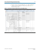
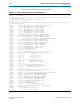
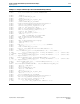
Table Of Contents
- Cyclone V Hard IP for PCI Express User Guide
- Contents
- 1. Datasheet
- 2. Getting Started with the Cyclone V Hard IP for PCI Express
- 3. Getting Started with the Avalon-MM Cyclone Hard IP for PCI Express
- Running Qsys
- Customizing the Cyclone VHard IP for PCI Express IP Core
- Adding the Remaining Components to the Qsys System
- Completing the Connections in Qsys
- Specifying Clocks and Interrupts
- Specifying Exported Interfaces
- Specifying Address Assignments
- Simulating the Example Design
- Simulating the Single DWord Design
- Understanding Channel Placement Guidelines
- Adding Synopsis Design Constraints
- Creating a Quartus II Project
- Compiling the Design
- Programming a Device
- 4. Parameter Settings for the Cyclone V Hard IP for PCI Express
- 5. Parameter Settings for the Avalon-MM Cyclone V Hard IP for PCI Express
- 6. IP Core Architecture
- Key Interfaces
- Protocol Layers
- Multi-Function Support
- PCI Express Avalon-MM Bridge
- Avalon-MM Bridge TLPs
- Avalon-MM-to-PCI Express Write Requests
- Avalon-MM-to-PCI Express Upstream Read Requests
- PCI Express-to-Avalon-MM Read Completions
- PCI Express-to-Avalon-MM Downstream Write Requests
- PCI Express-to-Avalon-MM Downstream Read Requests
- Avalon-MM-to-PCI Express Read Completions
- PCI Express-to-Avalon-MM Address Translation for Endpoints
- Minimizing BAR Sizes and the PCIe Address Space
- Avalon-MM-to-PCI Express Address Translation Algorithm
- Single DWord Completer Endpoint
- 7. IP Core Interfaces
- Cyclone V Hard IP for PCI Express
- Avalon-MM Hard IP for PCI Express
- Physical Layer Interface Signals
- Test Signals
- 8. Register Descriptions
- Configuration Space Register Content
- Altera-Defined Vendor Specific Extended Capability (VSEC)
- PCI Express Avalon-MM Bridge Control Register Access Content
- Avalon-MM to PCI Express Interrupt Registers
- PCI Express Mailbox Registers
- Avalon-MM-to-PCI Express Address Translation Table
- Root Port TLP Data Registers
- Programming Model for Avalon-MM Root Port
- PCI Express to Avalon-MM Interrupt Status and Enable Registers for Root Ports
- PCI Express to Avalon-MM Interrupt Status and Enable Registers for Endpoints
- Avalon-MM Mailbox Registers
- Correspondence between Configuration Space Registers and the PCIe Spec 2.1
- 9. Reset and Clocks
- 10. Transaction Layer Protocol (TLP) Details
- 11. Interrupts
- Interrupts for Endpoints Using the Avalon-ST Application Interface
- Interrupts for Root Ports Using the Avalon-ST Interface to the Application Layer
- Interrupts for Endpoints Using the Avalon-MM Interface to the Application Layer
- Interrupts for End Points Using the Avalon-MM Interface with Multiple MSI/MSI-X Support
- 12. Optional Features
- 13. Flow Control
- 14. Error Handling
- 15. Transceiver PHY IP Reconfiguration
- 16. SDC Timing Constraints
- 17. Testbench and Design Example
- Endpoint Testbench
- Root Port Testbench
- Chaining DMA Design Examples
- Test Driver Module
- Root Port Design Example
- Root Port BFM
- BFM Procedures and Functions
- 18. Debugging
- A. Transaction Layer Packet (TLP) Header Formats
- Additional Information

2–10 Chapter 2: Getting Started with the Cyclone V Hard IP for PCI Express
Qsys Design Flow
Cyclone V Hard IP for PCI Express December 2013 Altera Corporation
User Guide
■ pcie_reconfig_driver_0—This Avalon-MM master drives the Transceiver
Reconfiguration Controller. The pcie_reconfig_driver_0 is implemented in clear
text that you can modify if your design requires different reconfiguration
functions. After you generate your Qsys system, the Verilog HDL for this
component is available as: <working_dir>/<variant_name>/testbench/
<variant_name>_tb/simulation/submodules/altpcie_reconfig_driver.sv.
■ Transceiver Reconfiguration Controller—The Transceiver Reconfiguration
Controller dynamically reconfigures analog settings to improve signal quality. For
Gen1 and Gen2 data rates, the Transceiver Reconfiguration Controller must
perform offset cancellation and PLL calibration.
Generating the Testbench
Follow these steps to generate the chaining DMA testbench:
1. On the Qsys Generation tab, specify the parameters listed in Table 2–9.
2. Click the Generate button at the bottom of the Generation tab to create the
chaining DMA testbench.
Table 2–9. Parameters to Specify on the Generation Tab in Qsys
Parameter Value
Simulation
Create simulation model
None. (This option generates a simulation model you can include in your own
custom testbench.)
Create testbench Qsys system Standard, BFMs for standard Avalon interfaces
Create testbench simulation model Verilog
Synthesis
Create HDL design files for synthesis Turn this option on
Create block symbol file (.bsf) Turn this option on
Output Directory
Path pcie_qsys/gen1_x4_example_design
Simulation Leave this option blank
Testbench
(1)
pcie_qsys/gen1_x4_example_design/testbench
Synthesis
(2)
pcie_qsys/gen1_x4_example_design/synthesis
Note to Table 2–9:
(1) Qsys automatically creates this path by appending testbench to the output directory/.
(2) Qsys automatically creates this path by appending synthesis to the output directory/.