
User guide
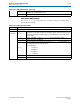
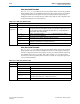
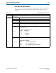
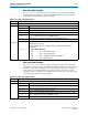
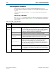
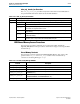
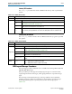
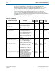
Table Of Contents
- Cyclone V Hard IP for PCI Express User Guide
- Contents
- 1. Datasheet
- 2. Getting Started with the Cyclone V Hard IP for PCI Express
- 3. Getting Started with the Avalon-MM Cyclone Hard IP for PCI Express
- Running Qsys
- Customizing the Cyclone VHard IP for PCI Express IP Core
- Adding the Remaining Components to the Qsys System
- Completing the Connections in Qsys
- Specifying Clocks and Interrupts
- Specifying Exported Interfaces
- Specifying Address Assignments
- Simulating the Example Design
- Simulating the Single DWord Design
- Understanding Channel Placement Guidelines
- Adding Synopsis Design Constraints
- Creating a Quartus II Project
- Compiling the Design
- Programming a Device
- 4. Parameter Settings for the Cyclone V Hard IP for PCI Express
- 5. Parameter Settings for the Avalon-MM Cyclone V Hard IP for PCI Express
- 6. IP Core Architecture
- Key Interfaces
- Protocol Layers
- Multi-Function Support
- PCI Express Avalon-MM Bridge
- Avalon-MM Bridge TLPs
- Avalon-MM-to-PCI Express Write Requests
- Avalon-MM-to-PCI Express Upstream Read Requests
- PCI Express-to-Avalon-MM Read Completions
- PCI Express-to-Avalon-MM Downstream Write Requests
- PCI Express-to-Avalon-MM Downstream Read Requests
- Avalon-MM-to-PCI Express Read Completions
- PCI Express-to-Avalon-MM Address Translation for Endpoints
- Minimizing BAR Sizes and the PCIe Address Space
- Avalon-MM-to-PCI Express Address Translation Algorithm
- Single DWord Completer Endpoint
- 7. IP Core Interfaces
- Cyclone V Hard IP for PCI Express
- Avalon-MM Hard IP for PCI Express
- Physical Layer Interface Signals
- Test Signals
- 8. Register Descriptions
- Configuration Space Register Content
- Altera-Defined Vendor Specific Extended Capability (VSEC)
- PCI Express Avalon-MM Bridge Control Register Access Content
- Avalon-MM to PCI Express Interrupt Registers
- PCI Express Mailbox Registers
- Avalon-MM-to-PCI Express Address Translation Table
- Root Port TLP Data Registers
- Programming Model for Avalon-MM Root Port
- PCI Express to Avalon-MM Interrupt Status and Enable Registers for Root Ports
- PCI Express to Avalon-MM Interrupt Status and Enable Registers for Endpoints
- Avalon-MM Mailbox Registers
- Correspondence between Configuration Space Registers and the PCIe Spec 2.1
- 9. Reset and Clocks
- 10. Transaction Layer Protocol (TLP) Details
- 11. Interrupts
- Interrupts for Endpoints Using the Avalon-ST Application Interface
- Interrupts for Root Ports Using the Avalon-ST Interface to the Application Layer
- Interrupts for Endpoints Using the Avalon-MM Interface to the Application Layer
- Interrupts for End Points Using the Avalon-MM Interface with Multiple MSI/MSI-X Support
- 12. Optional Features
- 13. Flow Control
- 14. Error Handling
- 15. Transceiver PHY IP Reconfiguration
- 16. SDC Timing Constraints
- 17. Testbench and Design Example
- Endpoint Testbench
- Root Port Testbench
- Chaining DMA Design Examples
- Test Driver Module
- Root Port Design Example
- Root Port BFM
- BFM Procedures and Functions
- 18. Debugging
- A. Transaction Layer Packet (TLP) Header Formats
- Additional Information
17–36 Chapter 17: Testbench and Design Example
BFM Procedures and Functions
Cyclone V Hard IP for PCI Express December 2013 Altera Corporation
User Guide
shmem_write
The
shmem_write
procedure writes data to the BFM shared memory.
shmem_read Function
The
shmem_read
function reads data to the BFM shared memory.
shmem_display Verilog HDL Function
The
shmem_display
Verilog HDL function displays a block of data from the BFM
shared memory.
Table 17–31. shmem_write Verilog HDL Task
Location altpcietb_bfm_driver_rp.v
Syntax
shmem_write(addr, data, leng)
Arguments
addr
BFM shared memory starting address for writing data
data
Data to write to BFM shared memory.
This parameter is implemented as a 64-bit vector.
leng
is 1–8 bytes. Bits 7 downto 0 are
written to the location specified by
addr
; bits 15 downto 8 are written to the
addr+1
location, etc.
leng
Length, in bytes, of data written
Table 17–32. shmem_read Function
Location altpcietb_bfm_driver_rp.v
Syntax
data:= shmem_read(addr, leng)
Arguments
addr
BFM shared memory starting address for reading data
leng
Length, in bytes, of data read
Return
data
Data read from BFM shared memory.
This parameter is implemented as a 64-bit vector.
leng
is 1- 8 bytes. If
leng
is less than 8
bytes, only the corresponding least significant bits of the returned data are valid.
Bits 7 downto 0 are read from the location specified by
addr
; bits 15 downto 8 are read from
the addr+1 location, etc.
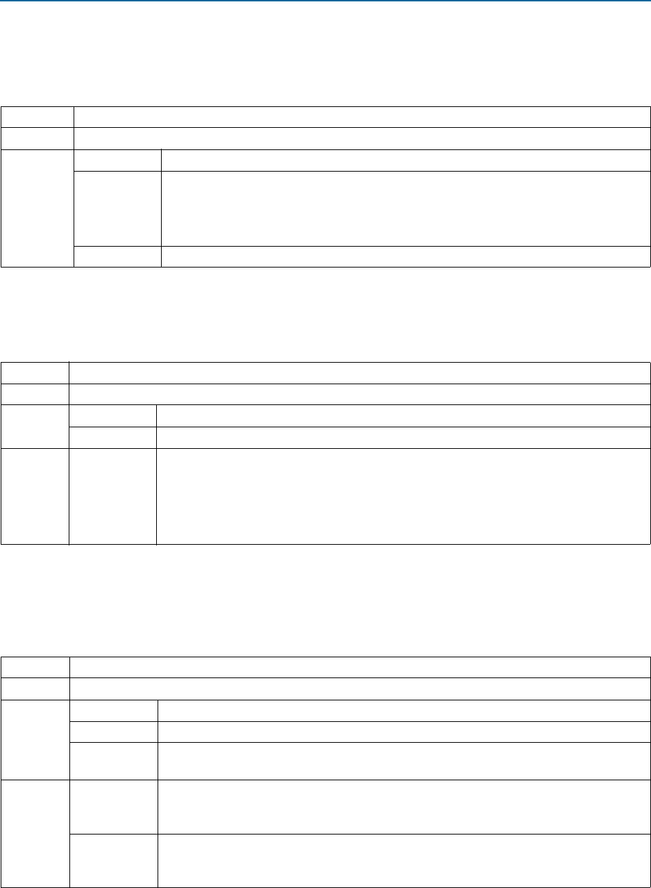
Table 17–33. shmem_display Verilog Function
Location altpcietb_bfm_driver_rp.v
Syntax Verilog HDL:
dummy_return:=shmem_display(addr, leng, word_size, flag_addr, msg_type);
Arguments
addr
BFM shared memory starting address for displaying data.
leng
Length, in bytes, of data to display.
word_size
Size of the words to display. Groups individual bytes into words. Valid values are 1, 2, 4, and
8.
flag_addr
Adds a <== flag to the end of the display line containing this address. Useful for marking
specific data. Set to a value greater than 2**21 (size of BFM shared memory) to suppress the
flag.
msg_type
Specifies the message type to be displayed at the beginning of each line. See “BFM Log and
Message Procedures” on page 17–37 for more information about message types. Set to one
of the constants defined in Table 17–36 on page 17–38.