
User guide


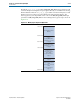
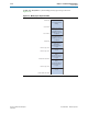
Table Of Contents
- Cyclone V Hard IP for PCI Express User Guide
- Contents
- 1. Datasheet
- 2. Getting Started with the Cyclone V Hard IP for PCI Express
- 3. Getting Started with the Avalon-MM Cyclone Hard IP for PCI Express
- Running Qsys
- Customizing the Cyclone VHard IP for PCI Express IP Core
- Adding the Remaining Components to the Qsys System
- Completing the Connections in Qsys
- Specifying Clocks and Interrupts
- Specifying Exported Interfaces
- Specifying Address Assignments
- Simulating the Example Design
- Simulating the Single DWord Design
- Understanding Channel Placement Guidelines
- Adding Synopsis Design Constraints
- Creating a Quartus II Project
- Compiling the Design
- Programming a Device
- 4. Parameter Settings for the Cyclone V Hard IP for PCI Express
- 5. Parameter Settings for the Avalon-MM Cyclone V Hard IP for PCI Express
- 6. IP Core Architecture
- Key Interfaces
- Protocol Layers
- Multi-Function Support
- PCI Express Avalon-MM Bridge
- Avalon-MM Bridge TLPs
- Avalon-MM-to-PCI Express Write Requests
- Avalon-MM-to-PCI Express Upstream Read Requests
- PCI Express-to-Avalon-MM Read Completions
- PCI Express-to-Avalon-MM Downstream Write Requests
- PCI Express-to-Avalon-MM Downstream Read Requests
- Avalon-MM-to-PCI Express Read Completions
- PCI Express-to-Avalon-MM Address Translation for Endpoints
- Minimizing BAR Sizes and the PCIe Address Space
- Avalon-MM-to-PCI Express Address Translation Algorithm
- Single DWord Completer Endpoint
- 7. IP Core Interfaces
- Cyclone V Hard IP for PCI Express
- Avalon-MM Hard IP for PCI Express
- Physical Layer Interface Signals
- Test Signals
- 8. Register Descriptions
- Configuration Space Register Content
- Altera-Defined Vendor Specific Extended Capability (VSEC)
- PCI Express Avalon-MM Bridge Control Register Access Content
- Avalon-MM to PCI Express Interrupt Registers
- PCI Express Mailbox Registers
- Avalon-MM-to-PCI Express Address Translation Table
- Root Port TLP Data Registers
- Programming Model for Avalon-MM Root Port
- PCI Express to Avalon-MM Interrupt Status and Enable Registers for Root Ports
- PCI Express to Avalon-MM Interrupt Status and Enable Registers for Endpoints
- Avalon-MM Mailbox Registers
- Correspondence between Configuration Space Registers and the PCIe Spec 2.1
- 9. Reset and Clocks
- 10. Transaction Layer Protocol (TLP) Details
- 11. Interrupts
- Interrupts for Endpoints Using the Avalon-ST Application Interface
- Interrupts for Root Ports Using the Avalon-ST Interface to the Application Layer
- Interrupts for Endpoints Using the Avalon-MM Interface to the Application Layer
- Interrupts for End Points Using the Avalon-MM Interface with Multiple MSI/MSI-X Support
- 12. Optional Features
- 13. Flow Control
- 14. Error Handling
- 15. Transceiver PHY IP Reconfiguration
- 16. SDC Timing Constraints
- 17. Testbench and Design Example
- Endpoint Testbench
- Root Port Testbench
- Chaining DMA Design Examples
- Test Driver Module
- Root Port Design Example
- Root Port BFM
- BFM Procedures and Functions
- 18. Debugging
- A. Transaction Layer Packet (TLP) Header Formats
- Additional Information
17–24 Chapter 17: Testbench and Design Example
Root Port BFM
Cyclone V Hard IP for PCI Express December 2013 Altera Corporation
User Guide
The
ebfm_cfg_rp_ep
procedure also sets up a
bar_table
data structure in BFM shared
memory that lists the sizes and assigned addresses of all Endpoint BARs. This area of
BFM shared memory is write-protected, which means any user write accesses to this
area cause a fatal simulation error. This data structure is then used by subsequent
BFM procedure calls to generate the full PCI Express addresses for read and write
requests to particular offsets from a BAR. This procedure allows the testbench code
that accesses the Endpoint Application Layer to be written to use offsets from a BAR
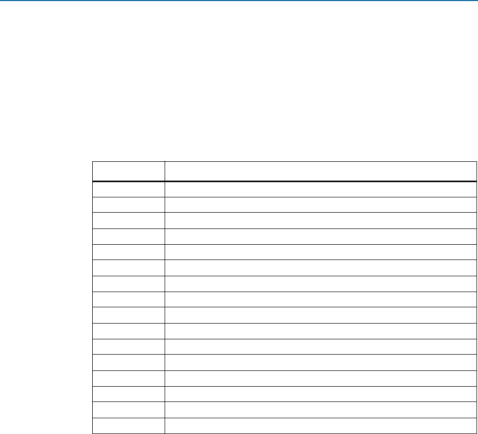
and not have to keep track of the specific addresses assigned to the BAR. Table 17–19
shows how those offsets are used.
The configuration routine does not configure any advanced PCI Express capabilities
such as the AER capability.
Table 17–19. BAR Table Structure
Offset (Bytes) Description
+0 PCI Express address in BAR0
+4 PCI Express address in BAR1
+8 PCI Express address in BAR2
+12 PCI Express address in BAR3
+16 PCI Express address in BAR4
+20 PCI Express address in BAR5
+24 PCI Express address in Expansion ROM BAR
+28 Reserved
+32 BAR0 read back value after being written with all 1’s (used to compute size)
+36 BAR1 read back value after being written with all 1’s
+40 BAR2 read back value after being written with all 1’s
+44 BAR3 read back value after being written with all 1’s
+48 BAR4 read back value after being written with all 1’s
+52 BAR5 read back value after being written with all 1’s
+56 Expansion ROM BAR read back value after being written with all 1’s
+60 Reserved